
Audio Codec '97

AC ‘97 Component Specification Revision 2.3 Rev 1.0
83
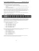
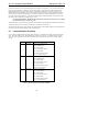
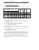
6.6.4 Modem DAC/ADC Level Control Registers (Index 46h – 4Ah)
Reg Name D15 D14 D13 D12 D11 D10 D9 D8 D7
D6
D5
D4
D3 D2 D1 D0 Default
46h Line 1 DAC/ADC Level Mute x x x DAC3 DAC2 DAC1 DAC0 Mute x x x ADC3 ADC2 ADC1 ADC0 8080h
48h Line 2 DAC/ADC Level Mute x x x DAC3 DAC2 DAC1 DAC0 Mute x x x ADC3 ADC2 ADC1 ADC0 8080h
4Ah Handset DAC/ADC Level Mute x x x DAC3 DAC2 DAC1 DAC0 Mute x x x ADC3 ADC2 ADC1 ADC0 8080h
These read/write registers control the modem AFE DAC and ADC levels. DAC levels are defined to be the same as
AC ‘97 Play Master Volume Register (2-6h minus 5
th
and 6
th
bits); ADC levels are defined to be the same as AC ‘97
Record Gain Registers (1C-1Eh).
The default value after cold or register reset for these registers (8080h) corresponds to 0 dB DAC attenuation with
mute on, 0 dB ADC gain/attenuation with mute on.
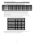
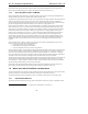
6.6.5 GPIO Pin Configuration Register (Index 4Ch)
Reg
Name
D15 D14 D13 D12 D11 D10 D9 D8 D7
D6
D5
D4
D3 D2 D1 D0 Default
4Ch GPIO Pin Config
(0 =output, 1=input)
GC15 GC14 GC13 GC12 GC11 GC10 GC9 GC8 GC7 GC6 GC5 GC4 GC3 GC2 GC1 GC0 FFFFh
The GPIO Pin Configuration is a read/write register that specifies whether a GPIO pin is configured for input (1) or
for output (0), and is accessed via the standard slot 1 and 2 command address/data protocols.
If a GPIO pin is implemented, the respective GCx bit should be read/writable and set to 1. If a GPIO is not
implemented, then the respective GCx bit should be read-only and set to 0. This informs the software how many
GPIO pins have been implemented. It is up to the AC ‘97 Digital Controller to send the desired GPIO pin value
over output slot 12 in the outgoing stream of the AC-link before configuring any of these bits for output.
The default value after cold or register reset for this register (FFFFh), is all pins configured as inputs.
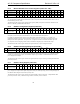
6.6.6 GPIO Pin Polarity/Type Register (Index 4Eh)
Reg Name D15 D14 D13 D12 D11 D10 D9 D8 D7
D6
D5
D4
D3 D2 D1 D0 Default
4Eh GPIO Pin Polarity/Type
(0 =low, 1=high active)
GP15 GP14 GP13 GP12 GP11 GP10 GP9 GP8 GP7 GP6 GP5 GP4 GP3 GP2 GP1 GP0 FFFFh
The GPIO Pin Polarity/Type is a read/write register that defines GPIO Input Polarity (0=Low, 1=High active) when
a GPIO pin is configured as an Input. It defines GPIO Output Type (0=CMOS, 1=OPEN-DRAIN) when a GPIO
pin is configured as an Output.
The default value after cold or register reset for this register (FFFFh) is all pins active high. Non-implemented GPIO
pins always return 1s.
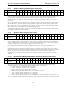
6.6.7 GPIO Pin Sticky Register (Index 50h)
Reg Name D15 D14 D13 D12 D11 D10 D9 D8 D7 D6 D5 D4 D3 D2 D1 D0 Default
50h GPIO Pin Sticky
(0 =not sticky, 1=sticky)
GS15 GS14 GS13 GS12 GS11 GS10 GS9 GS8 GS7 GS6 GS5 GS4 GS3 GS2 GS1 GS0 0000h
The GPIO Pin Sticky is a read/write register that defines GPIO Input Type (0=Non-Sticky, 1=Sticky) when a GPIO
pin is configured as an input. GPIO inputs configured as Sticky are cleared by writing a 0 to the corresponding bit of
the GPIO Pin Status Register 54h (see below), and by reset.
The default value after cold or register reset for this register (0000h) is all pins non-Sticky. Unimplemented GPIO
pins always return 0s. Sticky is defined as Edge sensitive, Non-Sticky as Level-sensitive.