
Audio Codec '97

AC ‘97 Component Specification Revision 2.3 Rev 1.0
84
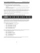
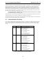
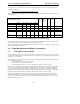
6.6.8 GPIO Pin Wake-up Mask Register (Index 52h)
Reg Name D15 D14 D13 D12 D11 D10 D9 D8 D7 D6 D5 D4 D3 D2 D1 D0 Default
52h GPIO Pin Wake-up
(0 =no int, 1=yes int)
GW15 GW14 GW13 GW12 GW11 GW10 GW9 GW8 GW7 GW6 GW5 GW4 GW3 GW2 GW1 GW0 0000h
The GPIO Pin Wake-up is a read/write register that provides a mask for determining if an input GPIO change will
generate a wake-up or GPIO_INT (0=No, 1=Yes). When the AC-Link is powered down (Register 26h PR4 = 1 for
Primary Codecs), a wake-up event will trigger the assertion of SDATA_IN (the AC-Link wake-up protocol is
defined in Section 3.5.2). When AC-link is powered up, a wake-up event will appear as GPIO_INT=1 on bit 0 of
input slot 12.
An AC-Link wake-up Interrupt is defined as a 0 to 1 transition on SDATA_IN when the AC-Link is powered down
(Register 26h PR4=1). GPIO bits that have been programmed as Inputs, Sticky and Pin Wake-up, upon transition
either (high-to-low) or (low-to-high) depending on pin polarity, will cause an AC-Link wake-up event (transition of
SDATA_IN from 0 to 1), if and only if the AC-Link was powered down.
The default value after cold or register reset for this register (0000h) defaults to all 0s specifying no wake-up event.
Non-implemented GPIO pins always returns 0s.
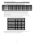
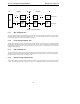
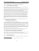
6.6.9 GPIO Pin Status Register (Index 54h)
Reg Name D15 D14 D13 D12 D11 D10 D9 D8 D7 D6 D5 D4 D3 D2 D1 D0 Default
54h GPIO Pin Status
(slot 12, bits 15-0)
GI15 GI14 GI13 GI12 GI11 GI10 GI9 GI8 GI7 GI6 GI5 GI4 GI3 GI2 GI1 GI0 xxxxh
The GPIO Status is a read/write register that reflects the state of all GPIO pins (inputs and outputs) on slot 12. The
value of all GPIO pin inputs and outputs comes in from the Codec every frame on slot 12, but is also available for
reading as GPIO Pin Status via the standard slot 1 and 2 command address/data protocols. GPIO inputs configured
as Sticky are cleared by writing a 0 to the corresponding bit of this Register 54h.
Bits corresponding to unimplemented GPIO pins should be forced to zero in this register and input slot 12.
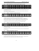
GPIO bits that have been programmed as Inputs and Sticky, upon transition either (high-to-low) or (low-to-high)
depending on Pin polarity, will cause the individual GI bit to go asserted 1, and remain asserted until a 0 is written to
that bit. The only way to set the desired value of a GPIO output pin is to set the control bit in output slot 12.
The default value, if configured as an input, after cold or register reset for this register is always the state of the
GPIO pin.
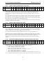
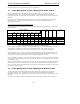
6.6.10 Miscellaneous Modem AFE Status and Control Register (Index 56h)
Reg Name D15 D14 D13 D12 D11 D10 D9 D8 D7 D6 D5 D4 D3 D2 D1 D0 Default
56h Miscellaneous Modem
AFE Stat/Ctrl
CID2 CID1 CIDR MLNK x HSB2 HSB1 HSB0 x L2B2 L2B1 L2B0 x L1B2 L1B1 L1B0 x000h
This read/write register defines the Loopback modes available for the modem line and handset ADCs/DACs
described in section 7.7. It also supports the optional CID bits described in Section 6.5.4.
• L1B2-0 controls Line 1 loopback modes (or disabled)
• L2B2-0 controls Line 2 loopback modes (or disabled)
• HSB2-0 controls Handset loopback modes (or disabled)
• MLNK controls a Secondary Modem Codec’s AC-link status (see below)
• CID1=1 indicates caller ID decode for Line 1 is supported
• CID2=1 indicates caller ID decode for Line 2 is supported
• CIDR=1 indicates that caller ID data is “raw” (demodulated but not decoded; includes seizure, marks, etc.)
AC ‘97 2.0 defined the modem MLNK bit as a flag which, when set, indicates to the modem Codec that the AC-link