
Audio Codec '97

AC ‘97 Component Specification Revision 2.3 Rev 1.0
97
9. Digital DC and AC Characteristics
9.1 DC Characteristics
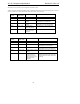
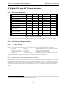
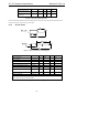
Parameter Symbol Min Typ Max Units
Digital Power Supply DVdd 3.135 3.3 3.465 V
Input voltage range V
in
-0.30 - DVdd + 0.30 V
Low level input voltage V
il
- - 0.35 x DVdd V
High level input voltage V
ih
0.65 x DVdd - - V
High level output voltage V
oh
0.90 x DVdd - - V
Low level output voltage V
ol
- - 0.10 x DVdd V
Input Leakage Current
(AC-link inputs)
- -10 - 10 µA
Output Leakage Current
(Hi-Z’d AC-link outputs)
- -10 - 10 µA
Input/Output Pin Capacitance - 7.5 pF
Table 52. 3.3 V DC Characteristics
AC ‘97 recommends new Controller and Codec designs support 3.3 V digital operation as specified in Table 52.
9.2 AC Timing Characteristics
9.2.1 Reset Timing
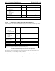
The AC ‘97 Architecture defines three types of reset that an AC ‘97 compatible Codec must comprehend:
1.
Cold reset RESET# Complete hardware reset; all registers default state
2.
Register reset - Audio write to 00h All audio registers default state
Register reset - Modem write to 3Ch Al modem registers default state
3.
Warm reset SYNC w/o BITCLK Re-activates AC-link; no change to register values
Registers should take their default values after Cold or Register reset, but not Warm reset.
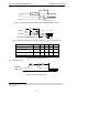
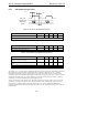
9.2.1.1 Recommended AC-link Cold Reset Behavior and Timing
As the popularity of OEM riser card audio increases (see the Communication and Networking Riser Specification),
so does the potential for motherboard audio and riser card audio electrical conflicts
17
. To minimize the potential for
damage from such conflicts, it is recommended that audio Codecs place their BIT_CLK and SDATA_IN pins in a
tri-state mode (instead of driving them low) while RESET# is active low. Figure 29 provides the recommended
timing:
17
However, for reliability, compatibility, and ease of use concerns, Intel does NOT recommend any configuration of
OEM riser card audio that disables motherboard audio and jacks.