
Front Panel I/O Connectivity Design Guide
Interface Board Design Guidelines
51
5.2 Front Panel I/O Interface Board Dimensions
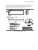
The front panel I/O interface board guideline defines an I/O aperture opening area that is
3.875 +/- 0.008 inch (98.43 +/- 0.20 mm) wide by 1.000 +/- 0.008 inch (25.40 +/- 0.20 mm) tall.
This area allows the use of stacked connectors on the board to maximize the amount of available
I/O space.
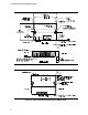
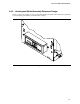
As shown in Figure 25 and Figure 26, the front panel I/O board guideline defines several keep-out
zones that are necessary for chassis interface features. A typical, 0.062-inch (1.57 mm) thick board
has a 0.100 to 0.108-inch (2.5 to 2.7 mm) keepout zone defined around the perimeter of the board,
and on both sides of the board. The keep-out zones provide reserved areas that can be used to
interface with a chassis-dependent front I/O housing or supporting structures. The keep-out zones
should be used as ground contact areas to increase ground return for EMI attenuation.
No components, connectors or other features should be placed within the keepout zones. The
maximum component height on the primary component side of the board (including board
thickness) is not to exceed 0.763 inch. (19.37 mm). The maximum component height on the
secondary side of the board is not to exceed 0.043 inches (1.09 mm). If the keepout zones are
violated, the board forfeits compatibility with the front panel I/O board-compliant chassis as
detailed in Figure 23 and Figure 24.
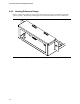
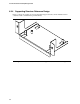
As shown in Figure 25 and Figure 26, the front panel I/O board guideline defines a board width of
3.500 +/- 0.008 inch. (88.90 +/- 0.20 mm), a minimum board depth of 1.500 inches (38.10 mm) and
a maximum board depth of 2.500 inches (63.50 mm). This variable board depth is intended to
retain flexibility for present and future technologies.
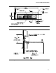
For the best EMI attenuation and proper grounding performance, board connector placement should
be limited as shown in Figure 23 and Figure 24 to allow enough clearance between the connectors
and the chassis opening for the I/O shield and/or front I/O housing structures. The indented notches
provided in the board definition may be used for a screw-less and/or clip retention method.
Refer to Figure 25 and Figure 26 for other front panel I/O interface board dimension and tolerance
recommendations. The connectors shown here are only examples.