
Front Panel I/O Connectivity Design Guide
Front Panel I/O Connectivity Design Guide
54
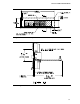
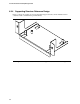
It is strongly recommended for the best EMI attenuation performance, paint should not be applied
within the 0.1 inches (2.54 mm) minimum keepout zone on the inside and outside surfaces of the
chassis front panel (Figure 27). Paint can prevent proper grounding of the I/O shield to the front
chassis panel. The following list shows some front panel I/O board highlights:
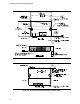
• Cutout size = 3.875 +/- 0.008 inches (98.43 +/- 0.20 mm) wide by 1.00 +/- 0.008 inches (25.4
+/- 0.20 mm) tall. See Figure 27.
• Distance from bottom of typical 0.062 inches (1.57 mm) thick board to bottom of I/O cutout
hole = 0.045 to 0.055 inches (1.14 to 1.39 mm). See Figure 27.
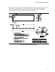
• Allowable thickness of the chassis front panel that the I/O shield can clip into is in the range
0.030 inches (0.76 mm) to 0.052 inches (1.32 mm).
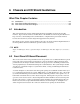
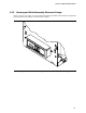
The interface board’s width is 3.500 +/- 0.008 inches (88.90 +/- 0.20 mm), its minimum depth is
1.500 inches (38.10 mm), and its maximum depth is 2.500 inches (63.50 mm), see Figure 25 and
Figure 26.
• The corners of the I/O aperture can be rounded to a maximum radius of 0.030 inches (0.76 mm)
as shown in Figure 27. This allowable rounding of the corners helps chassis manufactures
extend the life of their hard tooling while still complying with this guide.
• The 0.1 inches (2.5 mm) minimum keepout zone around the I/O aperture area is used in a front
panel I/O interface board compliant chassis (see Figure 27). This allows front panel I/O
interface board- compliant I/O shields to fit into front panel I/O interface board compliant
chassis. The keepout area is used for the shield attachment points. Avoid paint application in
the area.
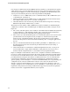
• The face of the Front Panel I/O board edge should be placed 0.053 +/- 0.010 inches (1.35 +/-
0.25 mm) from the inside of the chassis front panel I/O shield and/or chassis housing, as
defined in Figure 28.
• Chassis manufactures are not limited to an I/O shield implementation only. As long as the
chassis manufacturers comply with the definitions of this guide, they may choose to have
alternate methods of implementation, i.e., I/O shield or chassis dependent housing.
Figure 27 and Figure 28 detail the I/O connector zone. Compliance with this recommendation is
necessary to ensure enough clearance between the chassis aperture and the front panel I/O interface
board connectors for the I/O shield structure. This recommendation may be waived if the shield
provided with the board requires less than the recommended clearance. It is recommended that
system designers implement a universal design that would support a standard front panel I/O
aperture opening, as shown in Figure 27. To retain maximum flexibility, the exact positioning and
configuration of the connectors within the I/O connector zone is left to the discretion of the
designer. Connectors shown in Figure 27 are a reference design and are shown here only as an
example. Though it is not recommended for reasons of flexibility, a system designer may choose to
implement an integrated chassis housing and I/O shield to support and secure the front panel I/O
interface board. Then a supplied I/O shield may not be required.