IQ80960RM/RN Evaluation Platform Board Manual February 1999 Order Number: 273160-004
Information in this document is provided in connection with Intel products. No license, express or implied, by estoppel or otherwise, to any intellectual property rights is granted by this document.
Contents 1 Introduction ......................................................................................................................................1-1 i960® RM/RN I/O Processor and IQ80960RM/RN Features .....................................................1-3 Software Development Tools.....................................................................................................1-3 IxWorks Software Development Toolset.........................................................................
4.1 4.2 4.3 4.4 4.5 4.6 4.7 4.8 5 5.1 5.2 5.3 5.4 5.5 i960® RM/RN I/O Processor Overview ............................................................................................4-1 CPU Memory Map .....................................................................................................................4-2 Local Interrupts ..........................................................................................................................4-3 CPU Counter/Timers ........................
Figures 1-1 1-2 3-1 4-1 4-2 4-3 4-4 4-5 IQ80960RM/IQ80960RN Platform Functional Block Diagram ...................................................1-1 IQ80960RN Platform Physical Diagram ....................................................................................1-2 LED Register Bitmap .................................................................................................................3-8 i960® RM/RN I/O Processor Block Diagram..............................................................
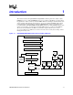
1 Introduction This manual describes the IQ80960RM and IQ80960RN evaluation platforms for Intel’s i960® RM/RN I/O processor. The i960 RM/RN I/O processors combine an 80960JT core with two PCI bus interfaces, as well as a memory controller, DMA channels, an interrupt controller interface, and an I2C serial bus. The difference between the two processors is that the 80960RN utilizes 64-bit primary PCI and secondary PCI buses while the 80960RM utilizes both a 32-bit primary and secondary PCI bus.
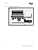
Introduction Figure 1-2.
Introduction 1.1 i960® RM/RN I/O Processor and IQ80960RM/RN Features The i960 RM/RN I/O processor serves as the main component of a high performance, PCI-based intelligent I/O subsystem. The IQ80960RM and IQ80960RN platforms allow the developer to connect PCI devices to the i960 RM/RN I/O processors using the four secondary PCI expansion connectors. The features of the IQ80960RM and IQ80960RN platforms are enumerated below and shown in Figure 1-1 and Figure 1-2.
Introduction 1.3 Tornado* for I20* Software Development Toolset Tornado for I20 is a complete toolset featuring an integrated development environment including a compiler, assembler, linker, and debugger. It also features a real-time operating system. 1.3.1 IxWorks* Real-Time Operating System The IQ80960RM/RN platforms are equipped with Wind River Systems, Inc.’s IxWorks*.
Introduction 1.4 CTOOLS Software Development Toolset Intel’s i960 processor software development toolset, CTOOLS, features advanced C/C++ - language compilers for the i960 processor family. CTOOLS development toolset is available for Windows* 95/NT-based systems and a variety of UNIX workstation hosts. These products provide execution profiling and instruction scheduling optimizations and include an assembler, a linker, and utilities designed for embedded processor software development. 1.4.
Introduction Refer to the SPI610 Reference Manual for JTAG emulation system installation and operation for both the Tornado and CTOOLS environment. Optionally, evaluation board serial port communications can be used for this communication link (see Section 1.3.3, “TORNADO Test and Debug Tools” on page 1-4). 1.6 About This Manual A brief description of the contents of this manual follows. 1-6 Chapter 1, “Introduction” Introduces the IQ80960RM and IQ80960RN Evaluation Board features.
Introduction 1.7 Notational-Conventions The following notation conventions are consistent with other i960 RM/RN I/O processor documentation and general industry standards. 1.8 # or overbar In code examples the pound symbol (#) is appended to a signal name to indicate that the signal is active. Normally inverted clock signals are indicated with an overbar above the signal name (e.g., RAS). Bold Indicates user entry and/or commands. PLD signal names are in bold lowercase letters (e.g., h_off, h_on).
Introduction 1.8.1 Intel Customer Electronic Mail Support For direct support from engineers specialing in i960® Microprocessor issues send e-mail in english to 960tools@intel.com. Questions and other messages may be posted to the Embedded Microprocessor Forum at http://support.intel.com/newsgroups/. 1.8.2 Intel Customer Support Contacts Contact Intel Corporation for technical assistance for the IQ80960RM/RN evaluation platform.
Introduction 1.8.3 Related Information To order printed manuals from Intel, contact your local sales representative or Intel Literature Sales (1-800-548-4725). Table 1-1.
Getting Started 2 This chapter contains instructions for installing the IQ80960RM/RN platform in a host system and, how to download and execute an application program using Wind River System’s IxWorks∗ or Intel’s CTOOLS software development toolsets. 2.1 Pre-Installation Considerations This section provides a general overview of the components required to develop and execute a program on the IQ80960RM/RN platform.
Getting Started 2.3 Hardware Installation Follow these instructions to get your new IQ80960RM/RN platform running. Be sure all items on the checklist were provided with your IQ80960RM/RN. Warning: 2.3.1 Static charges can severely damage the IQ80960RM/RN platforms. Be sure you are properly grounded before removing the IQ80960RM/RN platform from the anti-static bag. Battery Backup Battery backup is provided to save any information in SDRAM during a power failure.
Getting Started 4. If you have MON960 installed in the flash ROM, press on a terminal connected to the IQ80960RM/RN platform to bring up the MON960 prompt. MON960 automatically adjusts its baud rate to match that of the terminal at start-up. At baud rates other than 9600, it may be necessary to press several times. 2.
3 Hardware Reference 3.1 Power Requirements The IQ80960RM/RN platform draws power from the PCI bus. The power requirements of the IQ80960RM/RN platforms are shown in Table 3-1 and Table 3-2. The numbers do not include the power required by a PCI card(s) mounted on one or more of the IQ80960RM/RN platforms’ four expansion slots. Table 3-1. IQ80960RN Platform Power Requirements Voltage Typical Current Maximum Current +3.3 V 0 V* 0 V* +5 V 1.45 A 1.
Hardware Reference 3.2.1 SDRAM Performance The IQ80960RM/RN platform uses 72-bit SDRAM with ECC or 64-bit SDRAM without ECC. SDRAM allows zero data-to-data wait state operation at 66 MHz. The memory controller unit (MCU) of the i960® RM/RN I/O processor supports SDRAM burst lengths of four. A burst length of four enables seamless read/write bursting of long data streams, as long as the MCU does not cross the page boundary. Page boundaries are naturally aligned 2 Kbyte blocks.
Hardware Reference 3.2.2 Upgrading SDRAM The IQ80960RM/RN is equipped with 16 Mbytes of SDRAM with ECC inserted in the 168-pin DIMM socket. The memory may be expanded by inserting up to a 128 Mbyte module into the DIMM socket. The various memory combinations are shown in Table 3-4. Only 168-pin +3.3V SDRAM modules with or without ECC rated at 10 ns should be used on the IQ80960RM/RN platform. The column labeled ECC determines if that particular memory configuration can be used with ECC. Table 3-4.
Hardware Reference 3.4 Console Serial Port The console serial port on the IQ80960RM/RN platform, based on a 16C550 UART, is capable of operation from 300 to 115,200 bps. The port is connected to a phone jack-style plug on the IQ80960RM/RN platform. The DB25 to RJ-45 cable included with the IQ80960RM/RN can be used to connect the console port to any standard RS-232 port on the host system. The UART on the IQ80960RM/RN platform is clocked with a 1.
Hardware Reference 3.5.2 Interrupt and IDSEL Routing Table 3-6. Secondary PCI Bus Interrupt and IDSEL Routing 3.6 Connector IDSEL INTA# INTB# INTC# INTD# J11 SAD16 SINTA# SINTB# SINTC# SINTD# J12 SAD17 SINTB# SINTC# SINTD# SINTA# J13 SAD18 SINTC# SINTD# SINTA# SINTB# J14 SAD19 SINTD# SINTA# SINTB# SINTC# Battery Backup Battery backup is provided to save any information in SDRAM during a power failure.
Hardware Reference 3.8 Logic Analyzer Headers There are five logic analyzer connectors on the IQ80960RM/RN platform. The connectors are Mictor type, AMP part # 767054-1. Hewlett-Packard and Tektronix manufacture and sell interfaces to these connectors. The logic analyzer connectors allow for interfacing to the SDRAM and ROM buses along with secondary PCI arbitration signals. Table 3-7 shows the connectors and the pin assignments for each. Table 3-7.
Hardware Reference 3.9 JTAG Header The JTAG header allows debugging hardware to be quickly and easily connected to some of the IQ80960RM/RN processor’s logic signals. The JTAG header is a 16-pin header. A 3M connector (part number 2516-6002UG) is required to connect to this header. The pinout for the JTAG header is shown in Table 3-8. The header and connector are keyed using a tab on the connector and a slot on the header to ensure proper installation.
Hardware Reference 3.10 User LEDs The IQ80960RM/RN platform has a bank of eight user-programmable LEDs, located on the upper edge of the adapter board. These LEDs are controlled by a write-only register and used as a debugging aid during development. Software can control the state of the user LEDs by writing to the LED Register, located at E004 0000H. Each of the eight bits of this register correspond to one of the user LEDs.
Hardware Reference Table 3-11 lists the connectors and LEDs. Table 3-11.
i960® RM/RN I/O Processor Overview 4 This chapter describes the features and operation of the processor on the IQ80960RM/RN platform. For more detail, refer to the i960® RM/RN I/O Processor Developer’s Manual. Figure 4-1.
i960® RM/RN I/O Processor Overview 4.1 CPU Memory Map The memory map for the IQ80960RM/RN platform is shown in Figure 4-2. All addresses below 9002 0000H on the IQ80960RM/RN platform are reserved for various functions of the i960 RM/RN I/O processor, as shown on the memory map. Documentation for these areas, as well as the processor memory mapped registers at FF00 0000H and the IBR, can be found in the i960® RM/RN I/O Processor Developer’s Manual. Figure 4-2.
i960® RM/RN I/O Processor Overview 4.2 Local Interrupts The i960 RM/RN I/O processor is built around an 80960JT core, which has seven external interrupt lines designated XINT0# through XINT5# and NMI#. In the i960 RM/RN I/O processor, these interrupt lines are not directly connected to external interrupts, but pass through a layer of internal interrupt routing logic. Figure 4-3 shows the interrupt connections on the i960 RM/RN I/O processor.
i960® RM/RN I/O Processor Overview i960® RM/RN I/O Processor Interrupt Controller Connections P_INTA# Output P_INTB# Output P_INTC# Output P_INTD# Output Figure 4-3.
i960® RM/RN I/O Processor Overview 4.3 CPU Counter/Timers The i960 RM/RN I/O processor is equipped with two on-chip counter/timers which are clocked with the i960 RM/RN I/O processor clock signal. The i960 RM/RN I/O processor receives its clock from the primary PCI interface clock, generated by the motherboard. Most motherboards generate a 33 MHz clock signal, although the PCI specification requires a clock frequency between 0 and 33 MHz.
i960® RM/RN I/O Processor Overview 4.6 DMA Channels The i960 RM/RN I/O processor features three independent DMA channels, two of which operate on the primary PCI interface, whereas the remaining one operates on the secondary PCI interface. All three of the DMA channels connect to the i960 RM/RN I/O processor’s local bus and can be used to transfer data from PCI devices to memory on the IQ80960RM/RN platform. Support for chaining, and scatter/gather is built into all three channels.
i960® RM/RN I/O Processor Overview Figure 4-5 shows a simplified connection of the Application Accelerator to the i960 RM/RN I/O Processor Internal Bus. Figure 4-5. Application Accelerator Unit Application Accelerator Unit Data Queue Boolean Unit Packing/ Unpacking Unit 80960 Bus Interface 4.8 64-bit Internal Bus Performance Monitor Unit The Performance Monitoring features aid in measuring and monitoring various system parameters that contribute to the overall performance of the processor.
MON960 Support for IQ80960RM/RN 5 This chapter discusses a number of additions that have been made to MON960 to support the IQ80960RM/RN in an optional non-I2O capacity. For complete documentation on the operation of MON960, see the MON960 Debug Monitor User’s Guide. The IQ80960RM/RN evaluation platform ships with IxWorks* from Wind River Systems installed in flash firmware. To use CTOOLS and MON960 instead of IxWorks, you need to download MON960 into the onboard Flash.
MON960 Support for IQ80960RM/RN is given the ability to initialize the PCI configuration registers to values other than the default power-up values. Configuration Mode gives the user maximum flexibility to customize the way in which the i960 RM/RN I/O processor and IQ80960RM/RN platform appear to the PCI host configuration software. 5.2.
MON960 Support for IQ80960RM/RN 5.2.5 Primary PCI Interface Initialization The IQ80960RM/RN platform is a multi-function PCI device. On the primary PCI bus, two functions (from a PCI Configuration Space standpoint) are supported. • Function 0 is the PCI-to-PCI Bridge of the i960 RM/RN I/O processor, which optionally provides access capability between the primary PCI bus and the secondary PCI bus.
MON960 Support for IQ80960RM/RN By default, Primary Outbound Configuration Cycle parameters are not established. The ATU Configuration Register (ATUCR) is initialized to establish the operational parameters for the Doorbell Unit and ATU interrupts (both primary and secondary), and to enable the primary and secondary ATUs. The PCI host is responsible for allocating PCI address space (Memory, Memory Mapped I/O, and I/O), and assigning the PCI Base addresses for the IQ80960RM/RN platform. 5.2.
MON960 Support for IQ80960RM/RN 5.3 MON960 Kernel The MON960 Kernel (monitor) provides the IQ80960RM/RN user with a software platform on which application software can be developed and run. The monitor provides several features available to the IQ80960RM/RN user to speed application development.
MON960 Support for IQ80960RM/RN 5.4.2 PCI BIOS Routines MON960 includes PCI BIOS routines to aid application software initialization of the secondary PCI bus. The supported BIOS functions are described in the subsections that follow.
MON960 Support for IQ80960RM/RN 5.4.2.2 sysFindPCIDevice This function returns the location of PCI devices that have a specific Device ID and Vendor ID. Given a Vendor ID, a Device ID, and an Index, the function returns the Bus Number, Device Number, and Function Number of the Nth Device/Function whose Vendor ID and Device ID match the input parameters.
MON960 Support for IQ80960RM/RN 5.4.2.4 sysGenerateSpecialCycle This function allows for generation of PCI Special Cycles. The generated special cycle is broadcast on a specific PCI Bus in the system. PCI Special Cycles are not supported on the IQ80960RM/RN platform secondary PCI bus.
MON960 Support for IQ80960RM/RN 5.4.2.6 sysReadConfigWord This function allows the caller to read individual shorts (16 bits) from the configuration space of a specific device. The Register Number parameter must be a multiple of two (i.e., bit 0 must be set to “0”). Calling convention: int sysReadConfigWord ( int bus_number, int device_number, int function_number, int register_number, UINT16 /* 0,2,4,...
MON960 Support for IQ80960RM/RN 5.4.2.8 sysWriteConfigByte This function allows the caller to write individual bytes to the configuration space of a specific device. Calling convention: int sysWriteConfigByte ( int bus_number, int device_number, int function_number, int register_number, UINT8 /* 0,1,2,...,255 */ *data ); Return values: This function returns SUCCESSFUL when the indicated byte was written correctly, or ERROR when there is a problem with the parameters. 5.4.2.
MON960 Support for IQ80960RM/RN 5.4.2.10 sysWriteConfigDword This function allows the caller to write individual longs (32 bits) to the configuration space of a specific device. The Register Number parameter must be a multiple of four (i.e., bits 0 and 1 must be set to “0”). Calling convention: int sysWriteConfigDword ( int bus_number, int device_number, int function_number, int register_number, UINT32 /* 0,4,8,...
MON960 Support for IQ80960RM/RN 5.4.2.12 sysSetPCIIrq The PCI Interrupt routing fabric on the IQ80960RM/RN platform is not reconfigurable (fixed mapping relationships); therefore, this function is not supported. Calling convention: int sysSetPCIIrq ( int int int ); int_pin, irq_num, bus_dev Return values: This function always returns FUNC_NOT_SUPPORTED. 5.4.3 Additional MON960 Commands The following commands have been added to the UI interface of MON960 to support the IQ80960RM/RN platform. 5.4.3.
Bill of Materials A This appendix identifies all components on the IQ80960RN Evaluation Platform (Table A-1), and the IQ80960RM Evaluation Platform (Table A-2). 8 Table A-1.
Bill of Materials Table A-1.
Bill of Materials Table A-1. IQ80960RN Bill of Materials (Sheet 3 of 4) Item Qty Location Part Description Manufacturer Manufacturer Part # 31 1 R47 R/SM 1/10 W 5% 2.4 Kohm (0805) Dale CRCW0805242JT 32 2 R2, R57 R/SM 1/10 W 5% 2.7 Kohm (0805) Dale CRCW0805272JT 33 1 R19 R/SM 1/10 W 5% 330 ohm (0805) Dale CRCW0805331JT 34 1 R29 R/SM 1/10 W 5% 36 ohm (0805) Dale CRCW0805360JT 35 1 R17 R/SM 1/10 W 5% 470 ohm (0805) Dale CRCW 0805 471JT 36 2 R48, R49 R/SM 1/10 W 1% 4.
Bill of Materials Table A-1. IQ80960RN Bill of Materials (Sheet 4 of 4) Item A-4 Qty Location Part Description Manufacturer Manufacturer Part # 63 8 BT1, BT2, BT3, BT4, BT5, BT6, BT7, BT8 64 1 U15 HeatSink/Fan Assy 80960RM/RN Panasonic UDQFNBEOIF 65 1 C84 CAP SM, 0.
Bill of Materials Table A-2.
Bill of Materials Table A-2.
Bill of Materials Table A-2. IQ80960RM Bill of Materials (Sheet 3 of 5) Item Qty Location Part Description Manufacturer Manufacturer Part # 28 2 R50, R51 R/SM 1/10 W 5% 22 ohm (0805) Dale CRCW0805220JT 29 1 R34 R/SM 1/10 W 5% 22 Kohm (0805) Dale CRCW0805223JT 30 1 R37 R/SM 1/10 W 5% 24 ohm (0805) Dale CRCW0805240JT 31 1 R47 R/SM 1/10 W 5% 2.4 Kohm (0805) Dale CRCW0805242JT 32 1 R57 R/SM 1/10 W 5% 2.
Bill of Materials Table A-2.
Bill of Materials Table A-2.
Bill of Materials A-10 IQ80960RM/RN Evaluation Board Manual
Schematics B This appendix includes schematics for the IQ80960RN (Table B-1) and IQ80960RM (Table B-2). Table B-1. IQ80960RN Schematics List Page Schematic Title B-2 Decoupling and 3.
D C B A 1 +5V CAP0805 0.1uF CAP0805 0.1uF C48 2 1 2 CAP0805 0.1uF C116 2 1 CAP0805 0.1uF C113 2 1 CAP0805 0.1uF CAP0805 0.1uF C87 2 1 CAP0805 0.1uF C71 2 1 CAP0805 0.1uF C44 2 1 CAP0805 0.1uF CAP0805 0.1uF C69 2 1 CAP0805 0.1uF C73 2 1 CAP0805 0.1uF C111 2 1 CAP0805 0.1uF C108 2 1 CAP0805 0.1uF C114 2 1 CAP0805 0.1uF C115 2 1 CAP0805 0.1uF C112 2 1 CAP0805 0.1uF C109 2 1 CAP0805 0.1uF C105 2 1 CAP0805 0.1uF C50 2 1 CAP0805 0.1uF C59 2 1 CAP0805 0.1uF C49 2 1 C107 1 CAP0805 0.
D C L5 P_FRAME L1 PDEVSEL# M5 PSTOP# P_LOCK P_RST 1 U18 16 18 Q0 Q1 7 8 Q4 15 11 Q3 Q2 10 Q5 Q6 CY7B9910-7 CLK 1 REF FB 13 3 FS 23 TEST Q7 19 B7 M4 RST# PLOCK# A7 PGNT# P_GNT E6 P_REQ PREQ# P_PAR N3 P_STOP H3 P_IDSEL PPAR PIDSEL L2 PTRDY# P_TRDY L3 P_IRDY PIRDY# P_DEVSEL V4 P_C/BE7 P_C/BE6 P_C/BE5 P_C/BE4 P_C/BE3 P_C/BE2 PC/BE7# V3 PC/BE6# PAD62 PFRAME# V1 W5 PC/BE4# PC/BE5# H4 PC/BE3# PAD61 D6 PAD31 P_AD31 C6 PAD30 P_AD30 PAD59 A6 P_AD29 P
D C B 1 SCKE1 {06,11} SCKE0 {06,11} DCLKIN R50 1 C110 R51 1 1/10W 5% 22 2 1/10W 5% 22 2 18pF CAP0805 1 2 N29 N30 SA1 SA0 SBA0 SA0 SA1 SA2 SA3 SA4 SCE0 SDQM7 SCKE1 U30 M32 SDQM1 L29 SM2 SM1 SM0 SDQM0 SDQM2 U28 SDQM3 SM3 SDQM4 L28 SDQM6 M31 SDQM5 U29 V32 U32 SM4 SM5 SM6 SM7 M28 SCE1# SWE SCE1 T28 SCKE0 L32 M30 SWE# SCE0# SCAS SBA1 L30 N28 SA2 N32 SRAS P32 SA3 SA5 SA6 SCAS# P31 SA4 SRAS# P30 SA5 T30 P28 SA6 SA7 SA8 SA9 SA10 SA11 DC
D C B A 1 RAD {03,05} 3 4 5 6 7 8 9 11 RAD15 RAD14 RAD13 RAD12 RAD11 RAD10 RAD9 RALE RALE RAD3/RETRY RAD4/STEST RAD5 1D OC LE 8D 7D 6D 5D 4D 3D 2D 1D 4D LE 8D RCE0# 1 OC 11 9 6D 8 7D 7 6 5D 5 2D 4 3D 3 RAD6/RST_MODE# 2 1 2 RAD16 2 U2 18 19 12 13 14 15 16 17 18 19 14 Z4 8Q 12 7Q 13 6Q 3Q 17 16 4Q 5Q 15 2Q 1Q 8Q 7Q 6Q 5Q 4Q 3Q 2Q 1Q 2 JUMP1X2 1 74ABT573 U1 74ABT573 4 3 RAD11 RAD10 +5V 8 13 14 A10 15 ROMA12 ROMA11 ROMA
D C B A 1 SDRAM {03,06} 1 SM1 SM0 SCB7 SCB6 SCB5 SCB4 SCB3 SCB2 SCB1 SCB0 9 10 11 12 13 14 15 16 17 18 19 DQ10 DQ9 DQ8 DQ7 DQ6 DQ5 DQ4 DQ3 DQ2 DQ1 DQ0 2 SM2 8 DQ11 DQ55 DQ54 27 26 SA7 SA6 SA5 SA4 GND2 40 41 27 26 25 24 23 22 21 20 DQ39 DQ38 DQ37 DQ36 DQ35 DQ34 DQ33 DQ32 4 DQ56 28 SA8 28 DQ40 GND4 42 43 GND5 GND3 DQ57 29 SA9 29 DQ41 SA0 SA1 SA2 20 21 22 23 24 25 41 J11 GND4 42 43 GND5 GND3 GND2 40 DQ58 30 SA10 30 DQ42 39
1/10W 5% 1K R62 2 1 +3V REF CT C SCKE1 {03,11} SCKE0 {03,11} D SDRAM {03,05} RAM3V {01,04,11} 4 5 DQ2 DQ3 14 15 16 17 DQ12 DQ13 NC1 GND3 30 SCE0# 36 A4 39 BA1 A10 VCC5 E 42 CLK0 41 40 VCC4 38 SA10 SBA1 A6 37 A8 35 DCLK0 {03} GND4 A0 34 A2 33 32 SA6 SA8 CS0 31 NC3 SA4 SA2 SA0 29 SM1 M1 28 M0 SM0 WE VCC3 27 26 25 NC2 24 23 CB0 22 CB1 DQ15 DQ14 VCC2 DQ13 DQ12 DQ11 DQ10 DQ9 GND2 DQ8 DQ7 DQ6 DQ5 DQ4 VCC1 DQ3 DQ2 DQ1 J5 63 62 61 60 59
D C 1 AK19 SPAR S_PAR S_GNT5 S_GNT4 S_GNT3 S_GNT2 S_GNT1 S_GNT0 S_REQ5 S_REQ4 S_REQ3 S_REQ2 S_REQ1 AK12 S_PAR64 AK29 SGNT5# SPAR64 AM28 SGNT4# SAD61 SAD29 SAD30 SAD31 B AK28 SGNT3# SGNT0# AJ27 AJ29 AM26 SREQ5# AM27 AL28 SREQ4# SGNT1# AH28 SREQ3# SGNT2# AK27 SAD60 SAD28 SREQ2# SAD63 S_AD63 AH12 S_REQ0 SAD59 2 SAD27 AL26 SAD58 SAD26 AH27 SAD62 AM11 S_AD62 AK11 S_AD61 AJ11 S_AD60 AH11 S_AD59 AM10 S_AD58 SAD57 AL10 S_AD57 SAD55 SAD56 AH26 S
D C B A 1 C26 1 1 CLKB {02} CAP0805 0.01uF CAP0805 0.01uF C19 2 1 C18 2 1 STCK {09,10} N12V P33V {01,02,04,09} CLKA {02} CAP0805 0.01uF CAP0805 0.
D C B A 1 C2 1 1 CLKD {02} CAP0805 0.01uF CAP0805 0.01uF C3 2 1 2 STCK {08,10} N12V P33V {01,02,04,08} CLKC {02} CAP0805 0.01uF CAP0805 0.
D C B A 1 SPCI {05,07,08,09} 1 7 2 3 4 SREQ5# SACK64# SREQ64# 2 8 R31 2.7K RNC4R8P 5 6 5 6 1 7 8 SREQ4# R33 2.7K RNC4R8P 4 1 SREQ0# R38 2.7K 5 SREQ3# 4 SLOCK# 6 3 3 SPERR# 7 8 SREQ2# 2 SSERR# 2 1 SSTOP# RNC4R8P R45 2.7K 5 6 7 SREQ1# 4 SDEVSEL# 2 STRDY# 3 1 SFRAME# SIRDY# 5 4 STCK 8 6 3 STRST# RNC4R8P 7 2 R1 2.
D C B 1 C54 1 2 CAPT7343 10uF R60 PWR J13 FAN 1 FAN CONN 10 1/10W 5% 1 2 2 GND 3 R28 C74 1 2 1 1 1/10W 5% 1/10W 5% 1 2 1 2 CAPT3216 1uF 68K 1/10W 5% 1 2 +5V R27 R26 R34 2 13 6 11 7 16 1 100K 1/10W 5% 1 2 22K 1/10W 5% 1 2 5 BATTU14 FASTCHG GND PGM3 PGM2 PGM1 PGM0 TLO CC TEMP REF DRV R20 BATT+ MAX712 VLIMIT V+ THI R24 1K 1/10W 5% 1 2 0.01uF CAP0805 1 2 47K 1/10W 5% 1 2 0.01uF CAP0805 1 2 R25 C68 R53 C58 0.01uF CAP0805 1 2 4.7K 1/10W 5% 1 2 C55 4.
Schematics Table B-2. IQ80960RM Schematics List Page Schematic Title B-14 Decoupling and 3.
D C B A 1 +5V CAP0805 0.1uF C103 2 1 CAP0805 0.1uF C99 2 1 CAP0805 0.1uF C59 2 1 CAP0805 0.1uF C69 2 1 CAP0805 0.1uF CAP0805 0.1uF C66 2 1 CAP0805 0.1uF C62 2 1 CAP0805 0.1uF C49 2 1 CAP0805 0.1uF C73 2 1 CAP0805 0.1uF C48 2 1 2 CAP0805 0.1uF C116 2 1 CAP0805 0.1uF C113 2 1 CAP0805 0.1uF C111 2 1 CAP0805 0.1uF C108 2 1 CAP0805 0.1uF C114 2 1 CAP0805 0.1uF C115 2 1 CAP0805 0.1uF CAP0805 0.1uF C87 2 1 CAP0805 0.1uF C71 2 1 CAP0805 0.1uF C44 2 1 CAP0805 0.1uF CAP0805 0.
D C PTRDY# E6 P_LOCK P_GNT B7 P_RST A7 M4 1 U18 16 18 Q0 Q1 7 8 Q4 15 11 Q3 Q2 10 Q5 Q6 CY7B9910-7 CLK 1 REF FB 13 3 FS 23 TEST Q7 19 RST# PGNT# PLOCK# P_REQ P_IDSEL N3 P_PAR H3 PREQ# PPAR PIDSEL PSTOP# P_DEVSEL P_FRAME L3 P_IRDY L2 P_TRDY M5 P_STOP L1 PDEVSEL# PIRDY# L5 PFRAME# D6 PAD31 P_AD31 C6 PAD30 P_AD30 A6 PAD29 P_AD28 E5 P_AD27 G3 PAD28 P_AD26 G2 PAD27 B P_C/BE3 P_C/BE2 U15 i960RM PRIMARY PCI SIGNALS 2 6 3 5 7 2 4 8 1 R40 22 R55 22 R
D C B 1 SCKE1 {06,10} SCKE0 {06,10} DCLKIN C110 R51 1 1/10W 5% 22 2 1/10W 5% 22 R50 2 1 18pF CAP0805 1 2 N29 N30 SA1 SA0 SBA0 SA0 SA1 SA2 SA3 SA4 SCE1 SCE0 SDQM7 SCKE1 U30 M32 SDQM1 L29 SM2 SM1 SM0 SDQM0 SDQM2 U28 SDQM3 SM3 SDQM4 L28 SDQM6 M31 SDQM5 U29 V32 U32 SM4 SM5 SM6 SM7 M28 SCE1# SWE T28 SCKE0 L32 M30 SWE# SCE0# SCAS SBA1 L30 N28 SA2 N32 SRAS P32 SA3 SA5 SA6 SCAS# P31 SA4 SRAS# P30 SA5 T30 P28 SA6 SA7 SA8 SA9 SA10 SA11 DC
D C B RAD {03,05} 1 3 4 5 6 7 8 9 11 RAD15 RAD14 RAD13 RAD12 RAD11 RAD10 RAD9 RALE RALE RAD3/RETRY RAD4/STEST RAD5 1D OC LE 8D 7D 6D 5D 4D 3D 2D 1D 4D LE 8D U1 18 19 12 13 14 15 16 17 18 19 14 Z4 8Q 12 7Q 13 6Q 3Q 17 16 4Q 5Q 15 2Q 1Q 8Q 7Q 6Q 5Q 4Q 3Q 2Q 1Q 2 2 JUMP1X2 1 U2 74ABT573 RCE0# 1 OC 11 9 6D 8 7D 7 6 5D 5 2D 4 3D 3 RAD6/RST_MODE# 2 1 2 +5V ROMA20 40 A20 VPP 11 5 4 3 RAD12 RAD11 RAD10 14 A10 15 ROMA10 ROMA9
D C B A 1 SDRAM {03,06} 1 SM1 SM0 SCB7 SCB6 SCB5 SCB4 SCB3 SCB2 SCB1 SCB0 9 10 11 12 13 14 15 16 17 18 19 DQ10 DQ9 DQ8 DQ7 DQ6 DQ5 DQ4 DQ3 DQ2 DQ1 DQ0 2 SM2 8 DQ11 DQ55 DQ54 27 26 SA7 SA6 SA5 SA4 GND2 40 41 27 26 25 24 23 22 21 20 DQ39 DQ38 DQ37 DQ36 DQ35 DQ34 DQ33 DQ32 4 DQ56 28 SA8 28 DQ40 GND4 42 43 GND5 GND3 DQ57 29 SA9 29 DQ41 SA0 SA1 SA2 20 21 22 23 24 25 41 J11 GND4 42 43 GND5 GND3 GND2 40 DQ58 30 SA10 30 DQ42 39
+3V RESET C SCKE1 {03,10} SCKE0 {03,10} D 3 4 5 DQ1 DQ2 DQ3 15 16 17 DQ12 DQ13 21 SCB0 DQ15 DQ14 VCC2 DQ13 DQ12 DQ11 DQ10 DQ9 GND2 DQ8 DQ7 DQ6 DQ5 DQ4 VCC1 DQ3 DQ2 DQ1 NC1 GND3 36 39 BA1 A10 VCC5 42 CLK0 41 40 VCC4 38 SA10 SBA1 DCLK0 {03} A4 A6 37 A8 35 SA6 SA8 GND4 A0 34 A2 33 32 SA4 SA2 SA0 M1 CS0 31 NC3 30 29 SM1 SCE0# 28 M0 SM0 WE VCC3 27 SWE# 26 25 NC2 24 23 E J5 43 63 62 61 60 59 58 57 56 55 54 53 52 69 68 75 78 77
D C B 1 AJ27 AM27 AK28 AM28 AK29 AK19 SGNT2# SGNT3# SGNT4# SGNT5# SPAR S_PAR S_GNT5 S_GNT4 S_GNT3 S_GNT2 S_GNT1 S_AD30 SGNT1# S_GNT0 S_REQ5 AH26 S_AD31 SAD31 AJ29 AM25 SAD30 AM26 S_AD29 AK25 SAD29 SGNT0# S_AD28 AJ25 SAD28 SREQ5# S_REQ4 S_AD27 2 AH25 SAD27 S_AD26 AM24 SAD26 S_AD25 AL24 SAD25 S_REQ3 SAD24 AL28 SAD23 AH28 AK24 S_AD24 AM23 S_AD23 AK23 S_AD22 AJ23 S_AD21 SAD21 SREQ4# SAD19 SREQ3# U15 i960RM SECONDARY PCI SIGNALS SAD18 S_REQ2 SAD17 S_R
D C B A 1 SPCI CONN 2 SPCI CONN 1 1 2 2 CLKB {02} CAP0805 0.01uF CAP0805 0.01uF C19 2 1 C18 2 1 STCK {09} N12V P33V {01,02,04,09} CLKA {02} CAP0805 0.01uF CAP0805 0.
D C B A 1 SPCI CONN 4 SPCI CONN 3 1 C10 1 C2 1 CLKD {02} CAP0805 0.01uF CAP0805 0.01uF C3 2 1 2 STCK {08} N12V P33V {01,02,04,08} CLKC {02} CAP0805 0.01uF CAP0805 0.
D C B 1 10uF CAPT7343 1 2 C54 R60 PWR J13 FAN 1 FAN CONN 10 1/10W 5% 1 2 2 GND 3 R28 C74 1 2 1 1 1/10W 5% 1/10W 5% 1 2 1 2 CAPT3216 1uF 68K 1/10W 5% 1 2 +5V R27 R26 R34 2 13 6 11 7 16 1 100K 1/10W 5% 1 2 22K 1/10W 5% 1 2 5 BATTU14 FASTCHG GND PGM3 PGM2 PGM1 PGM0 TLO CC TEMP REF DRV R20 BATT+ MAX712 VLIMIT V+ THI R24 1K 1/10W 5% 1 2 0.01uF CAP0805 1 2 47K 1/10W 5% 1 2 0.01uF CAP0805 1 2 R25 C68 R53 C58 0.01uF CAP0805 1 2 4.7K 1/10W 5% 1 2 C55 4.
PLD Code C MODULE BATT //TITLE SDRAM Battery Backup Enable //PATTERN 101-1809-01 //REVISION //AUTHOR J. Neumann //COMPANY Cyclone Microsystems Inc. //DATE 10/30/97 //CHIP PALLV16V8Z-20JI // 1/20/98 Modify target device to PALLV16V8Z-20JI //Initial release.
Recycling the Battery D The IQ80960RM/RN platform contains four AA NiCd batteries. Each battery has the logo of the Rechargeable Battery Recycling Corporation (RBRC) stamped on it. The recycling fees have been prepaid on these batteries. Do not dispose of a rechargeable battery with regular trash in a landfill. Rechargeable batteries contain toxic chemicals and metals that are harmful to the environment. Improperly disposing of rechargeable batteries is also illegal.