
Datasheet

System on a Module Overview
August 2016 Intel® Joule™ Datasheet
Document number: 566641 rev. 1.0 Page 11
2.3.2 Method to provide +VSYS power to the module
The subject is covered in Section 3
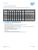
2.3.3 Required strapping of module pins
These module pin strappings must be implemented for boot during rising edge of PMIC_PWRGOOD (J6, pin 33).
2.3.4 BIOS installed onto module
The module requires a Basic Input Output System (BIOS) code to installed in the device firmware in order to complete the
boot and initialization process. The reference configuration loaded during module production can be overwritten with either
an updated, approved reference BIOS or a custom BIOS developed by other users, customers or partners.
Caution: Turning off the device during a BIOS update can cause data corruption and loss of functionality.
Warning: Installing a custom BIOS has the potential to change wireless radio operation in a ways that
take the module out of the regulatory compliance granted to the original production unit.
Consult local authorities for applicable testing and certification requirements for area of usage.
Regulatory Information for the Intel® Joule™ Compute Module
2.4 Expansion board recommendations
2.4.1 External EEPROM for multipurpose pin configuration data
An external EEPROM (recommend ST Microelectronics M24M02-DR* or equivalent) connected to I2C port 0 will hold a
specific configuration of the multipurpose pins. During boot, if the BIOS does not find an EEPROM device attached to I2C port
0, then the module will load the default configuration that is stored in BIOS.
2.4.2 Power button
Connect an active low power button to J6 pin 9 to trigger a reset or to power cycle the board.
2.4.3 DnX button
Connect an active high (VDD1) signal to J6, pin 78 to initiate a Download and Execute routine that will update the BIOS via
USB 2.0, port 0. This DnX button signal is the only way to initiate the Download and Execute update process.
2.4.4 Real time clock (RTC) backup power source
See section Section 9.1
2.4.5 UART debugging
Include a method to access UART port 2 on the module during boot to collect debug information as this is the only way to
access debug messages generated during the power on and boot sequences.
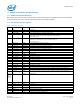
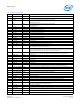
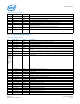
Table 4 Required strapping of module pins
Signal Name Location Default Requirement
GPIO_UART_TXD J6, pin 93 Internal 20k pull down Must be Hi-z or pulled down to GND when PMIC_PWRGOOD asserts
ISH_UART0_RTS J7, pin 11 Internal 20k pull up Must be Hi-z or pulled up to VDD1 when PMIC_PWRGOOD asserts
ISH_UART0_TXD J7, pin 15 Internal 20k pull down Must be Hi-z or pulled down to GND when PMIC_PWRGOOD asserts
SSP0_SPI_FS1 J7, pin 79 Internal 20k pull up Must be Hi-z or pulled up to VDD1 when PMIC_PWRGOOD asserts