
User's Manual

8XC196NP, 80C196NU USER’S MANUAL
10-16
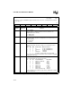
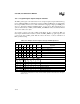
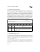
T1CONTROL
Address:
Reset State:
1F90H
00H
The timer 1 control (T1CONTROL) register determines the clock source, counting direction, and count
rate for timer 1.
7 0
CE UD M2 M1 M0 P2 P1 P0
Bit
Number
Bit
Mnemonic
Function
7 CE Counter Enable
This bit enables or disables the timer. From reset, the timers are
disabled and not free running.
0 = disables timer
1 = enables timer
6 UD Up/Down
This bit determines the timer counting direction, in selected modes (see
mode bits, M2:0).
0 = count down
1 = count up
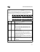
5:3 M2:0 EPA Clock Direction Mode Bits
These bits determine the timer clocking source and direction control
source.
M2 M1 M0 Clock Source Direction Source
000f/4 UD bit (T1CONTROL.6)
X 0 1 T1CLK pin
†
UD bit (T1CONTROL.6)
010f/4 T1DIR pin
011T1CLK pin
†
T1DIR pin
111quadrature clocking using T1CLK and T1DIR
†
If an external clock is selected, the timer counts on both the rising and
falling edges of the clock.
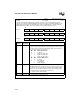
2:0 P2:0 EPA Clock Prescaler Bits
These bits determine the clock prescaler value.
P2 P1 P0 Prescaler Divisor Resolution
†
000divide by 1 (disabled) 160 ns
001divide by 2 320 ns
010divide by 4 640 ns
011divide by 8 1.28 µs
100divide by 16 2.56 µs
101divide by 32 5.12 µs
110divide by 64 10.24 µs
111divide by 128 (NU only) 20.48 µs
†
At f = 25 MHz. Use the formula on page 10-6 to calculate the resolution
at other frequencies.
Figure 10-8. Timer 1 Control (T1CONTROL) Register