
User's Manual

Intel
®
IXP42X Product Line of Network Processors and IXC1100 Control Plane Processor
September 2006 DM
Order Number: 252480-006US 197
Intel XScale
®
Processor—Intel
®
IXP42X product line and IXC1100 control plane processors
Please refer to “Instruction Latencies” on page 160 to get the instruction latencies for
various multiply instructions. The multiply instructions should be scheduled taking into
consideration these instruction latencies.
3.10.5.4 Scheduling SWP and SWPB Instructions
The SWP and SWPB instructions have a five-cycle issue latency. As a result of this
latency, the instruction following the SWP/SWPB instruction would stall for 4 cycles.
SWP and SWPB instructions should, therefore, be used only where absolutely needed.
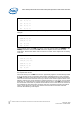
For example, the following code may be used to swap the contents of two memory
locations:
The code above takes nine cycles to complete. The rewritten code below, takes six
cycles to execute:
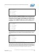
3.10.5.5 Scheduling the MRA and MAR Instructions (MRRC/MCRR)
The MRA (MRRC) instruction has an issue latency of one cycle, a result latency of two
or three cycles depending on the destination register value being accessed and a
resource latency of two cycles.
Consider the code sample:
The code shown above would incur a one-cycle stall due to the two-cycle resource
latency of an MRA instruction. The code can be rearranged as shown below to prevent
this stall.
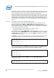
Similarly, the code shown below would incur a two-cycle penalty due to the three-cycle
result latency for the second destination register.
The stalls incurred by the code shown above can be prevented by rearranging the code:
; Swap the contents of memory locations pointed to by r0 and r1
ldr r2, [r0]
swp r2, [r1]
str r2, [r1]
; Swap the contents of memory locations pointed to by r0 and r1
ldr r2, [r0]
ldr r3, [r1]
str r2, [r1]
str r3, [r0]
mra r6, r7, acc0
mra r8, r9, acc0
add r1, r1, #1
mra r6, r7, acc0
add r1, r1, #1
mra r8, r9, acc0
mra r6, r7, acc0
mov r1, r7
mov r0, r6
add r2, r2, #1