
User's Manual

Intel
®
IXP42X Product Line of Network Processors and IXC1100 Control Plane Processor
September 2006 DM
Order Number: 252480-006US 355
Universal Asynchronous Receiver Transceiver (UART)—Intel
®
IXP42X product line and IXC1100
control plane processors
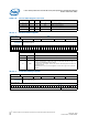
10.4.12 Scratch-Pad Register
This read/write register has no effect on the UART. The register is intended as a
scratch-pad register for use by the programmer.
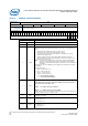
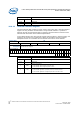
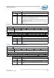
Register MSR
Bits Name Description
31:8 (Reserved)
7DCD
Data Carrier Detect: This bit is the complement of the Data Carrier Detect
(DCD#) input.
This bit is equivalent to bit OUT2 of the Modem Control register if LOOP in the
MCR is set to 1.
0 = DCD# pin is 1
1 = DCD# pin is 0
6RI
Ring Indicator: This bit is the complement of the ring Indicator (RI#) input.
This bit is equivalent to bit OUT1 of the Modem Control register if LOOP in the
MCR is set to 1.
0 = RI# pin is 1
1 = RI# pin is 0
5DSR
Data Set Ready: This bit is the complement of the Data Set Ready (DSR#)
input. This bit is equivalent to bit DTR of the Modem Control register if LOOP in
the MCR is set to 1.
0 = DSR# pin is 1
1 = DSR# pin is 0
4CTS
Clear to Send: This bit is the complement of the Clear to Send (CTS#) input.
This bit is equivalent to bit RTS of the Modem Control register if LOOP in the
MCR is set to 1.
0 = CTS# pin is 1
1 = CTS# pin is 0
3DDCD
Delta Data Carrier Detect:
0 = No change in DCD# pin since last read of MSR
1 = DCD# pin has changed state
2TERI
Trailing Edge Ring Indicator:
0 = RI# pin has not changed from 0 to 1 since last read of MSR
1 = RI# pin has changed from 0 to 1
1 DDSR
Delta Data Set Ready:
0 = No change in DSR# pin since last read of MSR
1 = DSR# pin has changed state
0 DCTS
Delta Clear To Send:
0 = No change in CTS# pin since last read of MSR
1 = CTS# pin has changed state
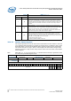
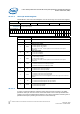
Register Name: SPR
Hex Offset Address: 0xC800 001C Reset Hex Value: 0x00000000
Register
Description:
Scratch Pad Register
Access: Read/Write.
31 87 0
(Reserved) SCR