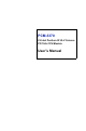
PCM-3370 LV Intel Pentium III/ ULV Celeron PC/104+ CPU Module User’s Manual
Copyright This document is copyrighted, © 2003. All rights are reserved. The original manufacturer reserves the right to make improvements to the products described in this manual at any time without notice. No part of this manual may be reproduced, copied, translated or transmitted in any form or by any means without the prior written permission of the original manufacturer. Information provided in this manual is intended to be accurate and reliable.
Packing List Before you begin installing your card, please make sure that the following materials have been shipped: • 1 PCM-3370 all-in one single board computer • 1 CD-ROM or disks for utility, drivers, and manual (in PDF format) • 1 warranty certificate • 1 2.5" IDE flat cable, 44-pin to 44-pin (product no. 1701440350) • 1 PS/2 keyboard & mouse cable (product no. 1700060202) • 2 serial port cables (product no. 1700100250) • 1 Y-cable external cable (product no.
Additional Information and Assistance Step 1. Visit the Advantech web site at www.advantech.com where you can find the latest information about the product. Step 2. Contact your distributor, sales representative, or Advantech's customer service center for technical support if you need additional assistance.
Safety Instructions 1. Read these safety instructions carefully. 2. Keep this User's Manual for later reference. 3. Disconnect this equipment from any AC outlet before cleaning. Use a damp cloth. Do not use liquid or spray detergents for cleaning. 4. For plug-in equipment, the power outlet socket must be located near the equipment and must be easily accessible. 5. Keep this equipment away from humidity. 6. Put this equipment on a reliable surface during installation.
Wichtige Sicherheishinweise 1. Bitte lesen sie Sich diese Hinweise sorgfältig durch. 2. Heben Sie diese Anleitung für den späteren Gebrauch auf. 3. Vor jedem Reinigen ist das Gerät vom Stromnetz zu trennen. Verwenden Sie Keine Flüssig-oder Aerosolreiniger. Am besten dient ein angefeuchtetes Tuch zur Reinigung. 4. Die NetzanschluBsteckdose soll nahe dem Gerät angebracht und leicht zugänglich sein. 5. Das Gerät ist vor Feuchtigkeit zu schützen. 6.
Caution! Danger of explosion if battery is incorrectly replaced. Replace only with the same or equivalent type recommended by the manufacturer. Dispose of used batteries according to the manufacturer’s instructions.
PCM-3370 User’s Manual viii
Content Chapter 1 General Information ........................................2 1.1 1.2 1.3 1.4 Introduction ....................................................................... 2 Features ............................................................................. 3 Specifications .................................................................... 4 Board Dimensions ............................................................. 6 Figure 1.1:Board Dimensions (Component Side)........... 6 Figure 1.
2.13.1 Ethernet connector (CN5)............................................. 19 2.13.2 Network boot ................................................................ 19 2.14 Watchdog timer configuration ........................................ 19 2.14.1 Watchdog timer action (JP2) ........................................ 19 Table 2.6:Watchdog Function J2 .................................. 19 2.15 2.16 USB connector (CN26,CN27)......................................... 20 Reset Connector (CN1) ............
Figure 4.10:Quit Setup Screen...................................... 42 Chapter 5 AGP 4X Setup.................................................44 5.1 Introduction ..................................................................... 44 5.1.1 5.1.2 5.1.3 5.1.4 5.2 Installation of the SVGA Driver ..................................... 46 5.2.1 5.2.2 5.2.3 5.2.4 5.2.5 5.3 Chapter Chipset .......................................................................... 44 Display memory..........................
B.17 B.18 B.19 B.20 B.21 B.22 B.23 B.24 B.25 B.26 B.27 CN17 KB/MS Connector .............................................. 105 CN18 ATX Power Connector ....................................... 105 CN19 Power Switch Connector .................................... 106 CN20 Negative Power Input ......................................... 106 CN21 Compact Flash Slot............................................. 106 CN22 RTC Connector................................................... 108 JP1 COMS Charge&Discharge..
CHAPTER 1 General Information This chapter gives background information on the PCM-3370.
Chapter 1 General Information 1.1 Introduction The PCM-3370 utilizes a PC/104+ form factor design that supports ULV Celeron 400/650 processors and LV Pentium III 800, 933 processors. This effective PC/104+ solution gives end users the choice of good, economical performance with the ULV Celeron series processors, or the impressive performance of the LV Pentium III series.
1.2 Features • All-in-one design simplifies system integration and increases system stability • Supports ULV Celeron 400/650 and LV Pentium III 800/933 processors. • Supports on-board features such as 1 x RS-232&1 x RS-232/422/485 with power and 2 x USB interfaces for external peripherals.
1.3 Specifications Standard SBC functions • CPU: On-board ULV Intel Celeron 400/650 (Fanless) / LV Pentium III 800/933 processor • BIOS: Award 256 KB Flash memory • Chipset: VIA 8606/TwisterT, VT82C686B • System memory: One SODIMM sockets accept 32 MB ~ 512MB SDRAM • Enhanced IDE interface: Supports up to two EIDE devices.
• Connection: On-board RJ-45 connector • Built-in boot ROM Mechanical and environmental • Max. power requirements:5V@2.4A for Intel Celeron ULV 400 @ 128M • Operating temperature: 0 ~ 60° C (32 ~ 140° F) • Dimensions (L x W): 96 mm x 115 mm (3.77" x 4.05") • Weight: 0.2Kg (0.
1.4 Board Dimensions Figure 1.
Figure 1.
PCM-3370 User’s Manual 8
CHAPTER 2 Installation This chapter explains how to set up the PCM-3370 hardware, including instructions on setting jumpers and connecting peripherals, switches and indicators. Be sure to read all the safety precautions before you begin the installation procedure.
Chapter 2 Installation 2.1 Jumpers The PCM-3370 has a number of jumpers that allow you to configure your system to suit your application. The table below lists the function of each of the board's connectors and jumpers Table 2.
JP2 Watchdog Timer JP3 PCI VIO SELECT JP4 COM1 RI Input Select JP5 COM2 RI Input Select 11 Chapter 2
2.2 Locating jumpers and connectors CN2 J P1 CN1 J P2 J P3 CN3 CN4 CN2 CN22 CN5 CN6 CN8 CN9 CN1 3 CN15 CN1 4 CN1 1 CN1 6 CN17 J P4 J P5 CN1 9 CN2 0 CN1 8 Figure 2.
BT1 CN21 DI MM1 Figure 2.2: Locating Connectors (Solder Side) 2.3 Setting Jumpers You configure your board to match the needs of your application by setting jumpers. A jumper is the simplest kind of electric switch. It consists of two metal pins and a small metal clip (often protected by a plastic cover) that slides over the pins to connect them. To ìcloseî a jumper you connect the pins with the clip. To ìopenî a jumper you remove the clip. Sometimes a jumper will have three pins, labeled 1, 2, and 3.
open closed closed 2-3 The jumper settings are schematically depicted in this manual as follows: open closed closed 2-3 A pair of needle-nose pliers may be helpful when working with jumpers. If you have any doubts about the best hardware configuration for your application, contact your local distributor or sales representative before you make any changes. Generally, you simply need a standard cable to make most connections. 2.4 CPU There are 4 CPU can be on-board.
Caution! Always ground yourself to remove any static charge before touching the PC board. Modern electronic devices are very sensitive to static electric charges. Use a grounding wrist strap at all times. Place all electronic components on a static-dissipative surface or in a static-shielded bag when they are not in the chassis. Warning! To avoid damaging the computer, always turn off the power supply before setting “Clear CMOS.” Set the jumper back to “3V Battery On” before turning on the power supply.
2.4.3 COM1 and COM2 RI Input Select (JP4, JP5) There is Ring input select jumper at COM1 and COM2. Table 2.4: COM1 and COM2 RI Input Select (JP4, JP5) JP4 COM1 RI Input Select Pin Function 1-2 RI * 2-3 VCC Table 2.5: COM1 and COM2 RI Input Select (JP4, JP5) JP5 COM2 RI Input Select Pin Function 1-2 RI * 2-3 VCC 2.5 SDRAM installation There are one on-board 144-pin SODIMM socket.
2.5.1 SODIMM DRAM You can install one DiMM (up to 512 MB). Caution! When installing SODIMM, make sure the module is oriented properly. Do not use excess force during installation. 2.6 Primary (2.5") IDE connector (CN12) The 44-pin IDE connector supports up to two 44-pin IDE interface devices, including CD-ROM drives, tape-backup drives, HDDs, etc. When connecting, make sure pin 1 of the connector is matched with pin of the device's connector.
2.9 Power connectors (CN15, CN18) 2.9.1 Main power connector (CN15) The power connection is a 8-pin connector requiring +5 V and +12 V power. It needs a cable (1703080104 for AT or 1703200380 for ATX) to connect AT/ATX power supply. 2.9.2 ATX standby power input connector (CN18) The power connection is a 3-pin connector requiring +5 V standby 2.10 Serial (COM1,COM2) (CN13,CN16) The PCM-3370 has a total of two on-board RS-232 serial ports, COM1 and COM2. They are COM1(RS-232) and COM2 (RS-232/422/485).
CN7 is 40-pin Hirose connector and CN10 is 20-pin Hirose connector. It can connect to a 36-bit TFT LCD panel. Pin assignments appear in the appendix. (For more information on LCD connection information between CN7 and CN10 and an LCD, refer to Chapter 3.) 2.12.3 Invert Power Connector (CN2) The PCM-33701F inverter power connector is a 5-pin boxheader. 2.13 Ethernet configuration The PCM-3370 is equipped with a high performance 32-bit PCI-bus Ethernet interface which is fully compliant with IEEE 802.
Table 2.6: Watchdog Function J2 2-3 IRQ11 2.15 USB connector (CN26,CN27) The PCM-3370 board provides two USB (Universal Serial Bus) interfaces which support plug and play and hot attach/detach for up to 127 external devices. The USB interfaces comply with USB specification Rev. 1.1 and are fuse protected. The USB interfaces are accessed through 10-pin (5x2) flat-cable connectors, CN9. You will need an adapter cable if you use a standard USB connector.
2.18.3 RTC Connector (CN22) PCM-3370F has a 2-pin boxheader real time clock connector.
PCM-3370 User’s Manual 22
CHAPTER 3 Software Configuration This chapter details the software configuration information. It shows you how to configure the card to match your application requirements. Award System BIOS will be covered in Chapter 4.
Chapter 3 Software Configuration 3.1 Introduction The PCM-3370 system BIOS and custom drivers are located in a 256 KB, 32-pin (JEDEC spec.) Flash ROM device, designated U23. A single Flash chip holds the system BIOS, VGA BIOS, and network Boot ROM image. The display can be configured via software. This method minimizes the number of chips and eases configuration. You can change the display BIOS simply by reprogramming the Flash chip. 3.
2. At the prompt, type AWDFLASH.EXE and press . The VGA configuration program will then display the following: Figure 3.1: VGA setup screen 3. At the prompt, enter the new BIN file which supports your display. When you are sure that you have entered the file name correctly press . 4. The screen will ask ìDo you want to save BIOS?î. If you change your mind or have made a mistake, press N to abort and end the setup procedure.
3.3 Connections for four standard LCDs Connections to Sharp LM64183P (640 x 480 DSTN MONO LCD) Table 3.
Table 3.2: PCM-3370 connection for PLANAR EL LCD (CN35) 7 LD3 13 P4 8 LD2 14 P5 9 CP2 35 SHFCLK 10 GND 33 GND 11 CP1 38 LP 12 GND 33 GND 13 S 36 FLM 14 GND 34 GND 15 GND 3 GND 16 GND 4 GND 17 VL 5 VCC 18 VL 6 VCC 19 VH 1 +12 V 20 VH 2 +12 V Connections to Toshiba LTM10C209A (640 x 480 TFT color LCD) Table 3.
Table 3.3: Toshiba LTM10C209A LCD (CN35) 13 G1 20 P11 14 G2 21 P12 15 GND 33 GND 16 G3 22 P13 17 G4 23 P14 18 G5 24 P15 19 GND 34 GND 20 ENAB 37 M 21 GND 34 GND 22 B0 11 P2 23 B1 12 P3 24 B2 13 P4 25 GND 39 GND 26 B3 14 P5 27 B4 15 P6 28 B5 16 P7 29 GND 39 GND 30 VDD 5 +5 V 31 VDD 6 +5 V Connections to Kyocera KCB6446BSTT-X5 (640 x 480 DSTN color LCD) Table 3.
Table 3.
3.4 Ethernet software configuration The PCM-3370’s on-board Ethernet interface supports all major network operating systems. To configure the medium type, to view the current configuration, or to run diagnostics, do the following: 1. Power the PCM-3370 on. Ensure that the RSET8139.EXE file is located in the working drive. 2. At the prompt type RSET8139.EXE and press . The Ethernet configuration program will then be displayed. 3.
CHAPTER 4 Award BIOS Setup This chapter describes how to set BIOS configuration data.
Chapter 4 Award BIOS Setup 4.1 System test and initialization These routines test and initialize board hardware. If the routines encounter an error during the tests, you will either hear a few short beeps or see an error message on the screen. There are two kinds of errors: fatal and non-fatal. The system can usually continue the boot up sequence with non-fatal errors.
4.2 Award BIOS setup Awardís BIOS ROM has a built-in Setup program that allows users to modify the basic system configuration. This type of information is stored in battery-backed CMOS RAM so that it retains the Setup information when the power is turned off. 4.2.1 Entering setup Power on the computer and press immediately. This will allow you to enter Setup. Figure 4.1: Setup Program Initial Screen 4.2.
online help information is displayed in the left bottom of the Menu screen. Figure 4.
4.2.3 BIOS features setup By choosing the BIOS FEATURES Setup option from the Initial Setup Screen menu, the screen below is displayed. This sample screen contains the manufacturerís default values for the PCM-3370. Figure 4.
4.2.4 Chipset features setup By choosing the CHIPSET FEATURES Setup option from the Initial Setup Screen menu, the screen below is displayed. This sample screen contains the manufacturerís default values for the PCM-3370. Figure 4.
4.2.5 Power management setup By choosing the POWER MANAGEMENT Setup option from the Initial Setup Screen menu, the screen below is displayed. This sample screen contains the manufacturerís default values for the PCM-3370. Figure 4.
4.2.6 PnP/PCI configuration setup By choosing the PnP/PCI CONFIGURATION option from the Initial Setup Screen menu, the screen below is displayed. This sample screen contains the manufacturerís default values for the PCM-3370. Figure 4.
4.2.7 Integrated peripherals By choosing the INTEGRATED PERIPHERALS option from the Initial Setup Screen menu, the screen below is displayed. This sample screen contains the manufacturerís default values for the PCM-3370. Figure 4.
4.2.8 Load Optimized Defaults BIOS LOAD OPTIMIZED DEFAULTS loads the default optimized system values directly from ROM. If the stored record created by the Setup program becomes corrupted (and therefore unusable), these defaults will load automatically when you turn the PCM-3370 on. Figure 4.8: Load Optimized Default BIOS screen 4.2.9 Set Password To change the password, choose the SET PASSWORD option form the Setup main menu and press . 1.
Confirm Password Enter the current password and press . 3. After pressing (ROM password) or the current password (user-defined), you can change the password stored in the CMOS. The password can be at most 8 characters long. Remember - to enable this feature, you must first select either Setup or System in the BIOS FEATURES SETUP. 4.2.10 Save & exit setup If you select this option and press , the values entered in the setup utilities will be recorded in the chipset's CMOS memory.
4.2.11 Quit without saving Selecting this option and pressing lets you Quit the Setup program without recording any new values or changing old ones. Figure 4.
CHAPTER 5 AGP 4X Setup The PCM-3370 features an onboard AGP 4X flat panel/VGA interface. This chapter provides instructions for installing and operating the software drivers on the included display driver diskette.
Chapter 5 AGP 4X Setup 5.1 Introduction The PCM-3370 has an onboard AGP flat panel/VGA interface. The specifications and features are described as follows: 5.1.1 Chipset The PCM-3370 uses a VIA Twister 8606T chipset from VIA Technology Inc. for its AGP/SVGA controller. It supports many popular LCD, and LVDS LCD displays and conventional analog CRT monitors. The VIA8606T VGA BIOS supports color TFT and DSTN LCD flat panel displays.
5.1.4 Dual/Simultaneous Display The PCM-3370 uses a VIA Twister VT8606T LCD controller that is capable of providing simultaneous dual view display of the same content on a flat panel and CRT. To set up dual view (simultaneus mode) under Windows 9x, Windows ME, Windows NT/2000/XP, follow these steps: Step 1. Open the Control panel, and select “Display”, “Settings”. Step 2. Select " CRT+LCD " or " CRT+TV " for dual view Step 3. Click “OK”. 1 Figure 5.
5.2 Installation of the SVGA Driver Complete the following steps to install the SVGA driver. Follow the procedures in the flow chart that apply to the operating system that you are using within your PCM-3370. Notes: 1. The windows illustrations in this chapter are intended as examples only. Please follow the listed steps, and pay attention to the instructions which appear on your screen. 2. For convenience, the CD-ROM drive is designated as "D" throughout this chapter. 5.2.1 Installation for Windows 95 1.
2. Choose the "Adapter" tab, then press the "Change..." button. 3. Press the "Have Disk" button.
4. Type in the path: D:\vga\VT8606\Win9x_Me 5. Select the highlighted item, and click the "OK" button.
6. "S3 GraphicsTwister" appears under the adapter tab. Click the "Apply" button, then the "OK" button. 7. Press “Yes” to reboot.
5.2.2 Installation for Windows 98/Me 1. Select "Start", "Settings", "Control Panel", "Display", and "Settings," then press the "Advanced..." button.
2. Select “Adapter,” then “Change.
3. Press “Next,” then “Display a list....” 4. Press the “Have disk...” button.
5. Insert the CD into the CD-ROM drive. Type in the path D:\vga\VT8606\Win9x_Me Then press “OK” 6. Select the highlighted item, then click “OK.
7. "S3 Graphics Twister"appears under the adapter tab. Click the "Apply" button. 8. Press “Yes” to reboot.
5.2.3 Installation for Windows NT Note: 1. Service Pack X (X = 3, 4, 5, 6,...) must be installed first, before you install the Windows NT VGA driver. Select "Start", "Settings", "Control Panel" and double click the "Display" icon.
2. Choose the "Settings" tab, and press the "Display Type" button.
3. Press the "Change..." button.
4. Click the "Have Disk..." button. 5. Type the path: D:\vga\VT8606\Win NT Press the "OK" button.
6. Select the highlighted item, and click the "OK" button. 7. Press "Yes" to proceed. 8. Press "OK" to reboot.
5.2.4 Installation for Windows 2000 1. Select "System", "Settings", "Control Panel" and double click the "system" icon.
2. Choose the "Video Controller (VGA Compatible)” button.
3. Choose the "Drive" button, press “Update Driver...” button.
4. Choose "Display a list of..." , then press “Next” button. 5. Choose “Display adapters”, press “Next” button.
6. Click the “Have Disk” button. 7. Type the path D:\vga\VT8606\Win2000 press the “OK” button.
8. Press “Finish" to reboot. 5.2.5 Installation for Windows XP 1. Select "System", "Settings", "Control Panel" and double click the "system" icon.
2. Choose “Hardware” and “Device Manager”, press “OK” button.
3. Choose “Video Controller (VGA Compatible), press “OK” button.
4. Choose "Driver”, “Update Driver”, press “OK” button. 5. Choose “Install from a list.....” , press “Next”.
6. Choose “Don’t search. I will....”, press “Next” button. 7. Choose “Display adapters”, press “Next” button.
8. Type the path D:\vga\VT8606\WinXP then press “OK” button. 9. Choose “S3 Graphics Twister + S3 Hotkey” then press “Next” button.
10. Press “Finish" to reboot. 5.3 Further Information For further information about the AGP/VGA installation in your PCM3370, including driver updates, troubleshooting guides and FAQ lists, visit the following web resources: VIA website: www.via.com.tw Advantech websites: www.advantech.com www.advantech.com.
PCM-3370 User’s Manual 72
CHAPTER 6 PCI Bus Ethernet Interface This chapter provides information on Ethernet configuration. • Introduction • Installation of Ethernet driver for - MS-DOS - Windows 3.
Chapter 6 PCI Bus Ethernet Interface 6.1 Introduction The PCM-3370 is equipped with a high-performance 32-bit Ethernet chipset which is fully compliant with IEEE 802.3 100 Mbps CSMA/CD standards. It is supported by major network operating systems. It is also both 100Base-T and 10Base-T compatible. The medium type can be configured via the PQ8139.exe program included on the utility disk. The Ethernet port provides a standard RJ-45 jack.
6.2.2 Installation for Windows 95 1. a. Select Start/Settings/Control Panel b. Double click "Network". 2. a. Click "Add" and prepare to install network functions.
3. a. Select the "Adapter" item to add the Ethernet card. 4. Click "Have Disk" to install the driver. 5. a. Insert the CD into the D: drive b. Fill in: D:\LAN\8139C\ c.
6. a. Choose the "Realtek" item b. Click "OK" 7. a. Make sure the configurations of relative items are set correctly b.
6.2.3 Installation for Windows 2000 Step 1.
Step 2.
Step 3. Step 4.
Step 5. Step 6.
Step 7. Step 8.
Step 9 6.2.4 Installation for Windows NT 1. a. Select Start/Settings/Control Panel. b. Double click "Network".
2. a. Choose the "Adapters" label. b. Click the "Add" button.
3 a. Press "Have Disk". 4. a. Type "D:". b. Press "OK". 5. a. Insert the CD into the D: drive. b. Fill in: D:\LAN\8139C\WINNT4 c. Press the "OK" button.
6. a. Choose the "Realtek" item. b. Press the "OK" button. 7. a. Make sure the configurations of relevant items are set correctly. b. Press the "OK" button to reboot.
6.3 Further information Realtek website: www.realtek.com Advantech websites:www.advantech.com www.advantech.com.
PCM-3370 User’s Manual 88
Appendix A Programming the Watchdog Timer The PCM-3370 is equipped with a watchdog timer that resets the CPU or generates an interrupt if processing comes to a standstill for whatever reason. This feature ensures system reliability in industrial standalone or unmanned environments.
Appendix A Programming the Watchdog Timer A.1 Programming the watchdog timer The following example show how you might program the watchdog timer in Assembly: 1. Watch Dog Timer Enable Port 404e Bit7 set "o" to enable PCM-3370 Watch Dog Timer Ex: Mov DX, 404e Mov AL, 7F Out DX, AL 2.
Appendix B Jumper Settings The PCM-3370 is equipped with a watchdog timer that resets the CPU or generates an interrupt if processing comes to a standstill for any reason. This feature ensures system reliability in industrial standalone or unmanned environments.
Appendix B PCM-3370F Jumper Settings Table B.1: Connectors 1. CN1 Reset Connect 2. CN2 Invert Power Connect 3. CN3 IR Connect CN4 FAN Connector 5. CN5 LAN Connector 6. CN6 422/485 Connect 7. CN7 40-pin LCD Port (24bit) 8. CN8 CRT Connect 9. CN9 USB Connector 10. CN10 20-Pin LCD Connector (36-bit) 11. CN11 PC/104+ Connector 12. CN12 44-Pin IDE Connector 13. CN13 COM2 RS232 Connector 14. CN14 LPT Connector 15. CN15 Power Connector 16.
B.1 CN1 Reset Connector Table B.2: CN1 Reset Connector Pin Pin name 1 Signal 2 GND 1 2 B.2 CN2 Inverter Power Connector Table B.
B.3 CN3 IR Connector Table B.4: IR Connector 1 +5V 2 NC 3 IRRX 4 GND 5 IRTX 5 4 3 2 B.4 CN4 FAN Connector Table B.
B.5 CN5 LAN Connector Table B.
B.6 CN6 422/485 Connector Table B.7: CN6 422/485 Connector 1 RX485- 2 RX485+ 3 TX485+ 4 TX485- 4 3 2 1 B.7 CN7 40-Pin LCD Port (24bit) Table B.8: CN7 40-Pin LCD Port (24bit) Pin Pin name Pin Pin name 1 LCD VDD(+5V) 2 LCD VDD(+5V) 3 GND 4 GND 5 LCD VDD(+3.3V) 6 LCD VDD(+3.
35 SHFCLK 36 FLM(V-SYNC) 37 M/(DE) 38 LP(H-SYNC) 39 ENABKL 40 ENVEE 1 3 37 3 9 2 4 38 4 0 B.8 CN8 CRT Connector Table B.
B.9 CN9 USB Connector Table B.
B.10 CN10 20-Pin LCD Connector (36-bit) Table B.11: CN10 20-Pin LCD Connector (36-bit) Pin Pinname Pin Pinname 1 GND 2 GND 3 PD24 4 PD25 5 PD26 6 PD27 7 PD28 8 PD29 9 PD30 10 PD31 11 PD32 12 PD33 13 PD34 14 PD35 15 GND 16 GND 17 NC 18 SPCLK 19 PCIRST 20 SPDAT 1 3 17 19 2 4 18 2 0 B.11 CN11 PC/104+ Connector Table B.
9 SD0 +12V LA17 DACKO* 10 IOCHRDY (KEY) MEMR* DRQ0 11 AEN SMEMW* MEMW* DACK5* 12 SA19 SMEMR* SD8 DRQ5 13 SA18 IOW* SD9 DACK6* 14 SA17 IOR* SD10 DRQ6 15 SA16 DACK3* SD11 DACK7* 16 SA15 DRQ3 SD12 DRQ7 17 SA14 DACK1* SD13 +5V DRQ1 SD14 MASTER* * low active 18 SA13 19 SA12 REFRESH* SD15 0V 20 SA11 SYSCLK (KEY) 0V 21 SA10 IRQ7 ---- ---- 22 SA9 IRQ6 ---- ---- 23 SA8 IRQ5 ---- ---- 24 SA7 IRQ4 ---- ---- 25 SA6 IRQ3 ---- ---- 26 S
B.12 CN12 44-Pin IDE Connector Table B.
B.13 CN13 COM2 RS232 Connector Table B.14: CN13 COM2 RS232 Connector Pin Pin name 1 DCD 2 DSR 3 RxD 4 RTS 5 TxD 6 CTS 7 DTR 8 RI 9 GND 10 N/C 1 3 5 7 9 2 4 6 8 10 B.14 CN14 LPT Connector Table B.
17 Data 7 18 GND 19 ACK- 20 GND 21 BUSY 22 GND 23 PaperEmpty 24 GND 25 SELECT 26 N/C 25 23 3 1 26 24 4 2 B.15 CN15 Power Conector Table B.
B.16 CN16 COM1 RS232 Connector Table B.
B.17 CN17 KB/MS Connector Table B.18: CN17 KB/MS Connector Pin Pin name 1 KB CLOCK 2 KB DATA 3 MS CLOCK 4 GND 5 +5V 6 MS DATA 6 5 4 3 2 1 B.18 CN18 ATX Power Connector Table B.
B.19 CN19 Power Switch Connector Table B.20: CN19 Power Switch Connector Pin Pin name 1 Signal 2 GND 1 2 B.20 CN20 Negative Power Input Table B.21: CN20 Negative Power Input Pin Pin name 1 -5V 2 GND 3 -12V 3 2 1 B.21 CN21 Compact Flash Slot Table B.
11 A08 12 A07 13 +5 V 14 A06 15 A05 16 A04 17 A03 18 A02 19 A01 20 A00 21 D00 22 D01 23 D02 24 *IOCS16 25 *CD2 26 *CD1 27 D11 28 D12 29 D13 30 D14 31 D15 32 *CS1 33 *VS1 34 *IORD 35 *IOWR 36 *WE 37 INTRQ 38 +5 V 39 *CSEL 40 *VS2 41 *RESER 42 IORDY 43 *INPACK 44 *REG 45 *DASP 46 *PDIAG 47 D08 48 D09 49 D10 50 GND * low active 107 Appendix B
B.22 CN22 RTC Connector Table B.23: CN22 RTC Connector Pin Pin name 1 Signal 2 GND 2 1 B.23 JP1 COMS Charge&Discharge Table B.24: JP1 COMS Charge&Discharge Pin Function 1-2 Charge * 2-3 Discharge Charge Discharge B.24 JP2 Watchdog Timer Table B.
B.25 JP3 PCI VIO Select Table B.26: JP3 PCI VIO Select Pin Function 1-2 VCC 2-3 VCC3 Default NULL * 1 2 3 1 2 3 VCC3 VCC B.26 JP4 COM1 RI Input Select Table B.
B.27 JP5 COM2 RI Input Select Table B.
Appendix C System Assignments • System I/O ports • DMA channel assignments • Interrupt assignments
Appendix C System Assignments C.1 System I/O ports Table C.1: System I/O ports Addr.
443 Watchdog timer ** default setting C.2 DMA channel assignments Table C.
C.3 Interrupt assignments Table C.
C.4 1st MB memory map Table C.4: 1st MB memory map Addr.
PCM-3370 User’s Manual 116