
Debug Port Design Guide for UP/DP Systems


DPDG for UP/DP Systems Order Number: 313373-001 15
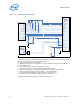
XDP Design Guide
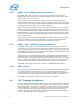
Notes:
A - These resistors will either be opens (if the processor has on-die termination) or 51
ohm 5% (if processor has no on-die termination).
B - This routing length is unconstrained.
C - These must be a maximum length of 1.5ns and must be length matched to within
50ps of one another but not to K.
E - Total length must be no more than 1.5ns. Each of these do not need to be length
matched.
F - Maximum trace routing of 200ps.
G - There are no trace routing requirements for this signal.
I - These traces lengths are determined by the driver and driver termination.
J - This resistance and routing is dependent on the front panel circuit receiver.
K - These must be no longer than 1.5ns and must be length matched to within 50ps of
one another but not to C.
M - There are no routing length requirements for this signal.
Z - Source termination method is defined by the clock driver.
All signals not noted except TDI and TDO are to be left NC
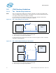
Figure 3-2. XDP DP Routing Overview
Proc 0
BPM0
BPM1
BPM2
BPM3
BPM4(PRDY)
BPM5(PREQ)
TMS
TCK
TRST#
RESET#
PWRGOOD
eXtended
Debug
Port
VCC_OBS_AB
OBSDATA_A3
OBSDATA_A2
OBSDATA_A1
OBSDATA_A0
OBSFN_A1
OBSFN_A0
TMS
TCK0
TRST#
HOOK0
HOOK4
HOOK5
HOOK6
HOOK7
XDPPr esent
GND
VCC_O BS_CD
OBSFN_B1
OBSFN_B0
OBSDATA_B3
OBSDATA_B2
OBSDATA_B1
OBSDATA_B0
1K 5%
Vtt
A
A
A
A
Front Panel Reset
XDP detect circuit
ClkOut
ClkOut #
Clock
Generator
G
C
C
C
C
C
C
E
G
F G
B
B
B
B
J
I
I
G
1.5- 3.3VDC
J
Vtt
K
K
K
K
K
K
51
5%
G
G
Proc 1
TRST#
TCK
TMS
BPM4( PRDY)
BPM5( PREQ)
BPM0
BPM1
BPM2
BPM3
E
G
51
5%
A
A
A
A
Vtt
M
M
M
M
E
B
Vtt
51
5%
Z
A
A
B
B
M
M
A
A