
Debug Port Design Guide for UP/DP Systems


DPDG for UP/DP Systems Order Number: 313373-001 17
XDP Design Guide
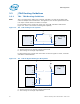
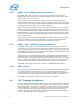
Notes:
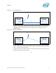
A - These traces have no specific routing requirements.
B - This routing has no length requirements.
The four-pin bypass jumper can completely isolate a processor socket whenever the
processor is not installed in the system. To include a processor load, place a jumper
across pins 2 - 1 as well as pins 4-3. To remove a processor load simply jumper pins 2-
4.
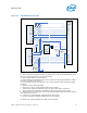
It is possible to replace the processor 4-pin bypass headers with Quick Switch* control
gates and use the socket occupied signal to control the bypass condition. This topology
is significantly different from the four-pin bypass header topology described earlier.
This topology will use fewer components compared to directly translating the headers
into Quick Switch* components. This topology also has the benefit of automatically
causing an open circuit between TDI and TDO if both processors of one of the TDI –
TDO chains are not occupied. These two bypass schemes have been designed to reduce
stubs and to limit the number of pull-ups on any one net to two.
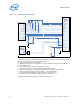
Quick Switch* components should be used for the MUX-DEMUX circuits in the figure
below. These MUX-DEMUX circuits can either be created using individual Quick Switch*
gates and inverters selectively used on the control signals, or through the use of Quick
Switch* 2:1 MUX-DEMUX similar to Fairchild Semiconductor* NC7SB3157 –
NC7SB3257 or equivalent.
Figure 3-5. TDI - TDO Jumpered Bypass Routing for DP Systems
51
5%
51
5%
B
Proc0
TDI
TDO
XDP Debug
Port
TDI
TDO
B
Proc1
TDI
TDO
51
5%
B
Vtt
`
Vtt
Vtt
1 2
3 4
AA
A
1 2
3 4
A
A
A
A