
Debug Port Design Guide for UP/DP Systems


XDP Design Guide
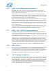
18 DPDG for UP/DP Systems Order Number: 313373-001
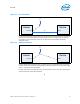
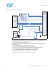
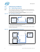
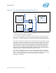
Notes:
A - These traces have no specific routing requirements.
B - This routing has no length requirements.
3.3.2 TCK0 Routing
Route a scan chain TCK to each of its loads in a daisy chain fashion and then terminate
with a 51 Ohm 5% resistor to GND at the processor end of the trace. The trace length
for this signal must be a maximum of 1.5ns. Any stub on these nets must be shorter
than 200ps. TCK0 should be routed to the CPU socket (UP) or both CPU sockets (DP).
Device chains other than processor chains are not described in this document. Do not
route TCK1 without contacting Intel for guidance.
3.3.3 TMS Routing Guidelines
TMS should be routed in a daisy chain fashion to each of the processors for a single
scan chain. CPU0 should be first in the route, followed by CPU1 for DP systems. The
TMS route for each scan chain should be terminated at the processor end with a 51
Ohm, 5% resistor to VTAP.
There is no trace length requirement for this signal.
3.3.4 TRSTn Routing Guidelines
This JTAG signal is routed as a daisy chain to all devices on all chains. There should be
a 51 Ohm 5% pull down resistor on the trace. The location of this resistor is
recommended to be near the last device in the chain with layout described in Section
2.1.1, “Termination Resistors” on page 10, but can be placed in other positions if
necessary for platform layout. The trace length of this signal is unimportant.
Figure 3-6. TDI - TDO Automatic Bypass for DP Systems
51
5%
51
5%
B
Proc0
SKTOCC#
TDI
TDO
XDP Debug
Port
TDI
TDO
B
Proc1
SKTOCC#
TDI
TDO
51
5%
B
Vtt
`
Vtt
Vtt
A
A
A
A
A
A
A
0
1
1
0
0
1
A
A
A