
Debug Port Design Guide for UP/DP Systems


DPDG for UP/DP Systems Order Number: 313373-001 19
XDP Design Guide
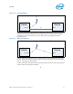
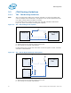
3.4 Run Control Routing Guidelines
Please see Section 3.7, “Observation Port Routing Guidelines” on page 21.
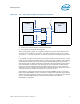
3.5 System Control Routing Guidelines
System Control operations report or manage the system power, scan, and reset states
of the target system. These signals are HOOK[0:7] on the XDP debug port. HOOK[1:3]
are generally left as no-connects.
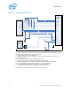
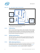
3.5.1 PWRGOOD (HOOK0) Routing Guidelines
Route a system PWRGOOD signal directly to the XDP HOOK0 pin. This signal is used to
indicate that the system’s power delivery subsystem has reached stability. This signal
must be asserted before the run control tool will attempt operations. The run control
tool will not drive PWRGOOD. The run control tool will use transitions on this signal as
triggering events. Please consult the system’s Platform Design Guidelines (PDG) for
termination information. If there is no PWRGOOD on system, pull this signal up to
1.0V-3.3V through a 1K-10K ohm resistor.
There are no trace length requirements for this signal.
3.5.2 Reserved (HOOK[1])
This signal is reserved. No connection to this signal are required.
3.5.3 Reserved (HOOK[2])
This signal is reserved. No connection to this signal is recommended.
3.5.4 Reserved (HOOK[3])
This signal is reserved. No connection to this signal is recommended.
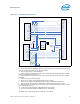
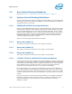
3.5.5 ITPCLK/ITPCLK# (HOOK[4:5]) Routing Guidelines
A copy of the processor Front Side Bus Clock (usually BCLK[0:1]) needs to be delivered
to the XDP by a system clock component. ITPCLK and ITPCLK# are used for noise and
synchronizer fault survivability, and as a frequency reference for run control operations
when enabled by the run control tool. Some run control and system interaction
operations may be disabled if ITPCLK is not connected or unavailable.
Route differentially from the system clock distribution component to the HOOK[4:5]
pins of XDP connector. Provide adequate source termination of the clock traces at the
clock driver. Route the signals using the specification of the driver. There are no length
matching requirements for this clock pair compared to any other signals in the target
system.
Due to the variations in processor nomenclature, BCLK[0:1] is sometimes denoted as
BCLK[p/n] respectively. Thus, BCLK[0] = BCLK[p] = ITPCLK = HOOK4 is the rising
edge for the beginning of every transaction. Conversely, BCLK[1] = BCLK[n] =
ITPCLK# = HOOK5.