
Debug Port Design Guide for UP/DP Systems

XDP Design Guide
20 DPDG for UP/DP Systems Order Number: 313373-001
3.5.6 RESET_IN# (HOOK6) Routing Guidelines
The RESET_IN# signal is an input to the run control tool from the front-side bus
RESET# signal. Run control tools will not drive RESET#; but uses this signal to sense
when a system reset has occurred.
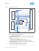
Route the front-side bus RESET# signal to the RESET_IN# pin through a 1Kohm
isolation resistor. Routing of this signal before the isolation resistor is left to the system
designers as part of the system design guides and datasheet. On the debug port side of
the isolation resistor, this signal has no length requirement.
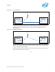
Rather than placing the isolation resistor within 200ps of the processor (as is shown in
Routing Overviews), the isolation resistor would ideally be placed to remove any stub
from the reset line by placing the isolation resistance pad directly at any point on the
RESET# signal line. There is no requirement from the point of view of the run control
tool but the system reset wired OR signal will have signal integrity issues with greater
than a minimum stub.
Special Note for systems with Dual Independent Bus: As both Resets in the system are
logically tied together (only a phase differential), the specific reset that HOOK6 is
connected to is not material. Route whichever is easier for the system.
3.5.7 RESET_OUT# (HOOK7) Routing Guidelines
The RESET_OUT# signal is an output from the run control tool to the system reset
control logic. The run control tool uses this signal to initiate a system reset. This reset
assertion must not cycle any power supplies on the target system nor may it alter the
PWRGOOD signal. The run control tool will drive this signal with a silicon switch closure
to ground when a debug reset is requested.
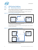
Route this signal to any point within the system reset topology that would initiate the
appropriate reset. Typical implementations route the RESET_OUT# signal to either a
reset controller FPGA; to an OR function within the front panel reset circuit; or directly
into the ICH signal SYS_RESET#. The pull up value and location is not critical to the run
control tool but may be to the receiver or other drivers if this signal is wire-ORed.
The RESET_OUT# signal name may be referred to as DBR# (Debug Port Reset).
3.5.8 XDP_Present
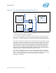
This optional steady-state output from the run control hardware indicates the presence
of an XDP style tool at the debug port. To use, the system will provide a pull-up
termination of 1K to 10K ohm to this signal. Termination voltage for this signal can be
to any voltage that is compatible with the receiver chosen by the platform design.
When XDP tool is present, the XDP tool will short this pin to ground.
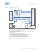
3.6 I2C* Routing Guidelines
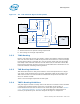
The I2C* interface from the XDP includes two pins – SDA and SCL. Route the XDP SDA
pin to the SDA signal of the SM Bus on the system. Route the XDP SCL pin to the SCL
signal of the SMBus on the system. The XDP I2C* interface is master only and cannot
be slave addressed. The XDP I2C* master can be connected to any multiple-master
I2C* bus within the target system that provides access to the hooks required for
validation and debug. The debug port has no additional requirements for termination
on these signals beyond the I2C* specifications.