
Debug Port Design Guide for UP/DP Systems
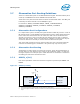

XDP Design Guide
22 DPDG for UP/DP Systems Order Number: 313373-001
3.7.4 OBSDATA_A[3:0]
3.7.4.1 Routing Guidelines
Route the CPU BPM[3:0]# point-to-point to the XDP OBSDATA_A[0:3] pins
(respectively). Designers should take careful note of the connectivity between pins for
these signals (see ).
These signals should be terminated at the processor socket: 51 Ohm, 5% to Vtt.
3.7.5 OBSDATA_B[3:0]
3.7.5.1 Routing Guidelines
Route the CPU BPM[3:0]# point-to-point to the XDP OBSDATA_B[0:3] pins
(respectively). Designers should take careful note of the connectivity between pins for
these signals (see ).
These signals should be terminated at the processor socket: 51 Ohm, 5% to Vtt.
3.8 Power
3.8.1 VCC_OBS Pins
The VCC_OBS_AB and VCC_OBS_CD pins are used by the XDP hardware to provide
termination voltage to the OBS interface. The JTAG signals are referenced off of the
VCC_OBS pins. Connect VCC_OBS_AB and VCC_OBS_CD to the VTAP voltage of the
processor. Decoupling capacitors are not required for these signals. Both connections
are required even in a UP / DP system.
Each of these pins draws ~200mA of current.
3.8.2 Ground
All XDP ground signals must be tied directly to the system ground with little to no trace
from the debug port.
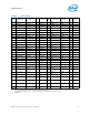
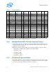
3.9 System Connection
The XDP connector is a Samtec* 60-pin BSH-030-01 series connector. Specific plating
types, locking clips, and alignment pins versions of this connector can be obtained from
Samtec*. The following table documents the pinout for this connector.