
Debug Port Design Guide for UP/DP Systems

DPDG for UP/DP Systems Order Number: 313373-001 29
XDP-SSA Design Guide
These lines in the past have had historical names associated with them. The OBS Port
historically has been referred to as the BPM#[0:5] pins.
Terminations on these signals vary based on processor. Check the documentation on
the last device on each signal to see if it has on-die termination (ODT). If it does not,
the signal requires a 51 ohm pull-ups to VTAP. Note that no termination is needed on
the debug port side of the transmission lines.
4.7.1 OBSFN_A[1:0]
The XDP-SSA OBSFN_A[1:0] routing guidelines are the same as those for the XDP0
OBSFN_x[1:0] routing guidelines (see Section 3.7.3, “OBSFN_x[1:0]” on page 21).
4.7.2 OBSDATA_A[3:0]
The XDP-SSA OBSDATA_A[3:0] routing guidelines are the same as those for the XDP0
OBSDATA_A[3:0] routing guidelines (see Section 3.7.4, “OBSDATA_A[3:0]” on
page 22).
4.8 Power
4.8.1 VCC_OBS Pins
The VCC_OBS_AB pins are used by the XDP-SSA hardware to provide termination
voltage to the OBS interface. The JTAG signals are referenced off of the VCC_OBS pins.
Connect VCC_OBS_AB to the VTAP voltage of the processor. Decoupling capacitors are
not required for these signals.
This pin draws ~200mA of current.
The XDP-SSA VCC_OBS routing guidelines are the same as those for the XDP0
VCC_OBS (see Section 3.8.1, “VCC_OBS Pins” on page 22).
4.8.2 Ground
All XDP-SSA ground signals must be tied directly to the system ground with little to no
trace from the debug port.
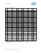
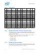
4.9 System Connection
The XDP-SSA connector is a Hirose* 31-pin DF9C-31S series connector or equivalent.
The following table documents the pinout for this connector.