
Debug Port Design Guide for UP/DP Systems


ITP700Flex Design Guide
36 DPDG for UP/DP Systems Order Number: 313373-001
5.4.1 Reserved (HOOK[0:3])
These signals are reserved. No connections to these signals are required.
5.4.2 ITPCLK/ITPCLK# (HOOK[4:5]) Routing Guidelines
A copy of the processor Front Side Bus Clock (usually BCLK[0:1]) needs to be delivered
to the debug port by a system clock component. ITPCLK and ITPCLK# are used for
noise and synchronizer fault survivability, and as a frequency reference for run control
operations when enabled by the run control tool.
Route differentially from the system clock distribution component to the HOOK[4:5]
pins of debug port connector. Provide adequate termination to the clock traces at the
clock driver. Some run control and system interaction operations may be disabled if
ITPCLK is not connected or unavailable.
The routing length of these signals should be equal to the length of BCLK to the
processor plus the length of the Obs_Data lengths.
Due to the variations in processor nomenclature, BCLK[0:1] is sometimes denoted as
BCLK[p/n] respectively. Thus, BCLK[0] = BCLK[p] = ITPCLK = HOOK4 is the rising
edge for the beginning of every transaction. Conversely, BCLK[1] = BCLK[n] =
ITPCLK# = HOOK5.
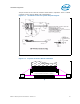
5.4.3 RESET_IN# (HOOK6) Routing Guidelines
The RESET_IN# signal is an input to the run control tool from front-side bus RESET#
signal. Run control tool will not drive RESET#; but uses this signal to sense when a
system reset has occurred.
Route RESET# from the processor to the RESET_IN# through a 150 ohm, 5% isolation
resistor. Routing of this signal before the isolation resistor is left to the system
designers as part of the system design guides. On the debug port side of the isolation
resistor, this signal has a length requirement of less than 1ns.
Rather than placing the isolation resistor within 200ps of the processor (as is shown in
Routing Overviews), the isolation resistor would ideally be placed to remove any stub
from the reset line by placing the isolation resistance pad directly on the RESET# signal
line. There is no requirement from the point of view of the run control tool but the
system reset wired OR signal will have signal integrity issues with larger than a
minimum stub.
Note that not all of the other system RESET routing is noted, only that needed by the
ITP700Flex. Consult the appropriate platform design guide for detailed requirements
for the processor RESET# signal.
5.4.4 RESET_OUT# (HOOK7) Routing Guidelines
The RESET_OUT# signal is an output from the run control tool to the system reset. The
run control tool uses this signal to initiate a system reset. This reset assertion must not
cycle any power supplies on the target system nor may it alter the PWRGOOD signal in
any way. The run control tool will drive this signal with a silicon switch closure to
ground when a debug reset is requested.
Route this signal to any point within the system reset topology that would initiate the
appropriate reset. Typical implementations route the RESET_OUT# signal to either a
reset controller FPGA; to an OR function within the front panel reset circuit; or directly