
Intel 64 and IA-32 Architectures Software Developers Manual Volume 3A, System Programming Guide, Part 1

10-4 Vol. 3A
MEMORY CACHE CONTROL
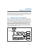
The L2 and L3 caches are unified data and instruction caches located on the
processor chip. Note that the L3 cache is only implemented on some Intel Xeon
processors.
• P6 family processors — The L1 cache is divided into two sections: one
dedicated to caching instructions (pre-decoded instructions) and the other to
caching data. The L2 cache is a unified data and instruction cache located on the
processor chip. P6 family processors do not implement a trace cache.
• Pentium processors — The L1 cache has the same structure as on P6 family
processors. There is no trace cache. The L2 cache is a unified data and instruction
cache external to the processor chip on earlier Pentium processors and
implemented on the processor chip in later Pentium processors. For Pentium
processors where the L2 cache is external to the processor, access to the cache is
through the system bus.
For processors based on Intel Core and Intel NetBurst microarchitectures, Intel Core
Duo, Intel Core Solo and Pentium M processors, the cache lines for the L1 and L2
caches (and L3 caches if supported) are 64 bytes wide. The processor always reads a
cache line from system memory beginning on a 64-byte boundary. (A 64-byte
aligned cache line begins at an address with its 6 least-significant bits clear.) A cache
line can be filled from memory with a 8-transfer burst transaction. The caches do not
support partially-filled cache lines, so caching even a single doubleword requires
caching an entire line.
The L1 and L2 cache lines in the P6 family and Pentium processors are 32 bytes wide,
with cache line reads from system memory beginning on a 32-byte boundary (5
least-significant bits of a memory address clear.) A cache line can be filled from
memory with a 4-transfer burst transaction. Partially-filled cache lines are not
supported.
The trace cache in processors based on Intel NetBurst microarchitecture is available
in all execution modes: protected mode, system management mode (SMM), and
real-address mode. The L1,L2, and L3 caches are also available in all execution
modes; however, use of them must be handled carefully in SMM (see Section 24.4.2,
“SMRAM Caching”).
The TLBs store the most recently used page-directory and page-table entries. They
speed up memory accesses when paging is enabled by reducing the number of
memory accesses that are required to read the page tables stored in system
memory. The TLBs are divided into four groups: instruction TLBs for 4-KByte pages,
data TLBs for 4-KByte pages; instruction TLBs for large pages (2-MByte or 4-MByte
pages), and data TLBs for large pages. The TLBs are normally active only in protected
mode with paging enabled. When paging is disabled or the processor is in real-
address mode, the TLBs maintain their contents until explicitly or implicitly flushed
(see Section 10.9, “Invalidating the Translation Lookaside Buffers (TLBs)”).
The store buffer is associated with the processors instruction execution units. It
allows writes to system memory and/or the internal caches to be saved and in some
cases combined to optimize the processor’s bus accesses. The store buffer is always
enabled in all execution modes.