
Intel 64 and IA-32 Architectures Software Developers Manual Volume 3B, System Programming Guide Part 2
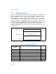
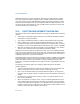
Table Of Contents
- Chapter 18 Debugging and Performance Monitoring
- 18.1 Overview of Debug Support Facilities
- 18.2 Debug Registers
- 18.3 Debug Exceptions
- 18.4 Last Branch Recording Overview
- 18.5 Last Branch, Interrupt, and Exception Recording (Intel® Core™2 Duo and Intel® Atom™ Processor Family)
- 18.6 Last Branch, Interrupt, and Exception Recording (Intel® Core™i7 Processor Family)
- 18.7 Last Branch, Interrupt, and Exception Recording (Processors based on Intel NetBurst® Microarchitecture)
- 18.7.1 CPL-Qualified Branch Trace Mechanism
- 18.7.2 MSR_DEBUGCTLA MSR
- 18.7.3 LBR Stack for Processors Based on Intel NetBurst Microarchitecture
- 18.7.4 Monitoring Branches, Exceptions, and Interrupts
- 18.7.5 Single-Stepping on Branches, Exceptions, and Interrupts
- 18.7.6 Branch Trace Messages
- 18.7.7 Last Exception Records
- 18.7.8 Branch Trace Store (BTS)
- 18.8 Last Branch, Interrupt, and Exception Recording (Intel® Core™ Solo and Intel® Core™ Duo Processors)
- 18.9 Last Branch, Interrupt, and Exception Recording (Pentium M Processors)
- 18.10 Last Branch, Interrupt, and Exception Recording (P6 Family Processors)
- 18.11 Time-Stamp Counter
- 18.12 Performance Monitoring Overview
- 18.13 Architectural Performance Monitoring
- 18.14 Performance Monitoring (Intel® Core™ Solo and Intel® Core™ Duo Processors)
- 18.15 Performance Monitoring (Processors based on Intel® Core™ Microarchitecture)
- 18.16 Performance Monitoring (Processors based on Intel® Atom™ Microarchitecture)
- 18.17 Performance Monitoring for Processors based on Intel® Microarchitecture (Nehalem)
- 18.18 Performance Monitoring (Processors Based on Intel NetBurst microarchitecture)
- 18.18.1 ESCR MSRs
- 18.18.2 Performance Counters
- 18.18.3 CCCR MSRs
- 18.18.4 Debug Store (DS) Mechanism
- 18.18.5 DS Save Area
- 18.18.6 Programming the Performance Counters for Non-Retirement Events
- 18.18.6.1 Selecting Events to Count
- 18.18.6.2 Filtering Events
- 18.18.6.3 Starting Event Counting
- 18.18.6.4 Reading a Performance Counter’s Count
- 18.18.6.5 Halting Event Counting
- 18.18.6.6 Cascading Counters
- 18.18.6.7 EXTENDED CASCADING
- 18.18.6.8 Generating an Interrupt on Overflow
- 18.18.6.9 Counter Usage Guideline
- 18.18.7 At-Retirement Counting
- 18.18.8 Precise Event-Based Sampling (PEBS)
- 18.18.9 Operating System Implications
- 18.19 Performance Monitoring and Intel Hyper- Threading Technology in Processors Based on Intel NetBurst Microarchitecture
- 18.20 Counting Clocks
- 18.21 Performance Monitoring, Branch Profiling and System Events
- 18.22 Performance Monitoring and Dual-Core Technology
- 18.23 Performance Monitoring on 64-bit Intel Xeon Processor MP with Up to 8-MByte L3 Cache
- 18.24 Performance Monitoring on L3 and Caching Bus Controller sub-systems
- 18.25 Performance Monitoring (P6 Family Processor)
- 18.26 Performance Monitoring (Pentium Processors)
- Chapter 19 Introduction to Virtual-Machine Extensions
- Chapter 20 Virtual-Machine Control Structures
- 20.1 Overview
- 20.2 Format of the VMCS Region
- 20.3 Organization of VMCS Data
- 20.4 Guest-State Area
- 20.5 Host-State Area
- 20.6 VM-Execution Control Fields
- 20.6.1 Pin-Based VM-Execution Controls
- 20.6.2 Processor-Based VM-Execution Controls
- 20.6.3 Exception Bitmap
- 20.6.4 I/O-Bitmap Addresses
- 20.6.5 Time-Stamp Counter Offset
- 20.6.6 Guest/Host Masks and Read Shadows for CR0 and CR4
- 20.6.7 CR3-Target Controls
- 20.6.8 Controls for APIC Accesses
- 20.6.9 MSR-Bitmap Address
- 20.6.10 Executive-VMCS Pointer
- 20.6.11 Extended-Page-Table Pointer (EPTP)
- 20.6.12 Virtual-Processor Identifier (VPID)
- 20.7 VM-Exit Control Fields
- 20.8 VM-Entry Control Fields
- 20.9 VM-Exit Information Fields
- 20.10 Software Access to the VMCS and Related Structures
- 20.11 Using VMCLEAR to Initialize a VMCS Region
- Chapter 21 VMX Non-Root Operation
- 21.1 Instructions That Cause VM Exits
- 21.2 APIC-Access VM Exits
- 21.3 Other Causes of VM Exits
- 21.4 Changes to Instruction Behavior in VMX Non- Root Operation
- 21.5 APIC Accesses That Do Not Cause VM Exits
- 21.6 Other Changes in VMX Non-Root Operation
- 21.7 Features Specific to VMX Non-Root Operation
- Chapter 22 VM Entries
- 22.1 Basic VM-Entry Checks
- 22.2 Checks on VMX Controls and Host-State Area
- 22.3 Checking and Loading Guest State
- 22.3.1 Checks on the Guest State Area
- 22.3.1.1 Checks on Guest Control Registers, Debug Registers, and MSRs
- 22.3.1.2 Checks on Guest Segment Registers
- 22.3.1.3 Checks on Guest Descriptor-Table Registers
- 22.3.1.4 Checks on Guest RIP and RFLAGS
- 22.3.1.5 Checks on Guest Non-Register State
- 22.3.1.6 Checks on Guest Page-Directory-Pointer-Table Entries
- 22.3.2 Loading Guest State
- 22.3.3 Clearing Address-Range Monitoring
- 22.3.1 Checks on the Guest State Area
- 22.4 Loading MSRs
- 22.5 Event Injection
- 22.6 Special Features of VM Entry
- 22.6.1 Interruptibility State
- 22.6.2 Activity State
- 22.6.3 Delivery of Pending Debug Exceptions after VM Entry
- 22.6.4 VMX-Preemption Timer
- 22.6.5 Interrupt-Window Exiting
- 22.6.6 NMI-Window Exiting
- 22.6.7 VM Exits Induced by the TPR Shadow
- 22.6.8 Pending MTF VM Exits
- 22.6.9 VM Entries and Advanced Debugging Features
- 22.7 VM-Entry Failures During or After Loading Guest State
- 22.8 Machine Checks During VM Entry
- Chapter 23 VM Exits
- 23.1 Architectural State Before a VM Exit
- 23.2 Recording VM-Exit Information and Updating VM-Entry Control Fields
- 23.3 Saving Guest State
- 23.4 Saving MSRs
- 23.5 Loading Host State
- 23.5.1 Loading Host Control Registers, Debug Registers, MSRs
- 23.5.2 Loading Host Segment and Descriptor-Table Registers
- 23.5.3 Loading Host RIP, RSP, and RFLAGS
- 23.5.4 Checking and Loading Host Page-Directory-Pointer-Table Entries
- 23.5.5 Updating Non-Register State
- 23.5.6 Clearing Address-Range Monitoring
- 23.6 Loading MSRs
- 23.7 VMX Aborts
- 23.8 Machine Check During VM Exit
- Chapter 24 Support for Address Translation
- 24.1 Virtual Processor Identifiers (VPIDs)
- 24.2 Extended Page Tables (EPT)
- 24.3 Caching Translation Information
- Chapter 25 System Management
- 25.1 System Management Mode Overview
- 25.2 System Management Interrupt (SMI)
- 25.3 Switching Between SMM and the Other Processor Operating Modes
- 25.4 SMRAM
- 25.5 SMI Handler Execution Environment
- 25.6 Exceptions and Interrupts Within SMM
- 25.7 Managing Synchronous and Asynchronous System Management Interrupts
- 25.8 NMI Handling While in SMM
- 25.9 SMM Revision Identifier
- 25.10 Auto HALT Restart
- 25.11 SMBASE Relocation
- 25.12 I/O Instruction Restart
- 25.13 SMM Multiple-Processor Considerations
- 25.14 Default Treatment of SMIs and SMM with VMX Operation and SMX Operation
- 25.15 Dual-Monitor Treatment of SMIs and SMM
- 25.15.1 Dual-Monitor Treatment Overview
- 25.15.2 SMM VM Exits
- 25.15.3 Operation of an SMM Monitor
- 25.15.4 VM Entries that Return from SMM
- 25.15.4.1 Checks on the Executive-VMCS Pointer Field
- 25.15.4.2 Checks on VM-Execution Control Fields
- 25.15.4.3 Checks on VM-Entry Control Fields
- 25.15.4.4 Checks on Guest Non-Register State
- 25.15.4.5 Loading Guest State
- 25.15.4.6 VMX-Preemption Timer
- 25.15.4.7 Updating the Current-VMCS and SMM-Transfer VMCS Pointers
- 25.15.4.8 VM Exits Induced by VM Entry
- 25.15.4.9 SMI Blocking
- 25.15.4.10 Failures of VM Entries That Return from SMM
- 25.15.5 Enabling the Dual-Monitor Treatment
- 25.15.6 Activating the Dual-Monitor Treatment
- 25.15.7 Deactivating the Dual-Monitor Treatment
- 25.16 SMI and Processor Extended State Management
- Chapter 26 Virtual-Machine Monitor Programming Considerations
- 26.1 VMX System Programming Overview
- 26.2 Supporting Processor Operating Modes in Guest Environments
- 26.3 Managing VMCS Regions and Pointers
- 26.4 Using VMX Instructions
- 26.5 VMM Setup & Tear Down
- 26.6 Preparation and Launching a Virtual Machine
- 26.7 Handling of VM Exits
- 26.8 Multi-Processor Considerations
- 26.9 32-Bit and 64-Bit Guest Environments
- 26.10 Handling Model Specific Registers
- 26.11 Handling Accesses to Control Registers
- 26.12 Performance Considerations
- Chapter 27 Virtualization of System Resources
- 27.1 Overview
- 27.2 Virtualization Support for Debugging Facilities
- 27.3 Memory Virtualization
- 27.4 Microcode Update Facility
- Chapter 28 Handling Boundary Conditions in a Virtual Machine Monitor
- Appendix A Performance-Monitoring Events
- A.1 Architectural Performance-Monitoring Events
- A.2 Performance Monitoring Events for Intel® Intel® Core™i7 Processor Family
- A.3 Performance Monitoring Events for Intel® Xeon® Processor 5200, 5400 Series and Intel® Core™2 Extreme ProcessorS QX 9000 Series
- A.4 Performance Monitoring Events for Intel® Xeon® Processor 3000, 3200, 5100, 5300 Series and Intel® Core™2 Duo ProcessorS
- A.5 Performance Monitoring Events for Intel® Atom™ ProcessorS
- A.6 Performance Monitoring Events for Intel® Core™ Solo and Intel® Core™ Duo ProcessorS
- A.7 Pentium 4 and Intel Xeon Processor Performance-Monitoring Events
- A.8 Performance Monitoring Events for Intel® Pentium® M ProcessorS
- A.9 P6 Family Processor Performance- Monitoring Events
- A.10 Pentium Processor Performance- Monitoring Events
- Appendix B Model-Specific Registers (MSRs)
- B.1 Architectural MSRs
- B.2 MSRs In the Intel® Core™ 2 Processor Family
- B.3 MSRs In the Intel® Atom™ Processor Family
- B.4 MSRs In the Intel® Microarchitecture (Nehalem)
- B.5 MSRs In the Pentium® 4 and Intel® Xeon® Processors
- B.6 MSRs In Intel® Core™ Solo and Intel® Core™ Duo Processors
- B.7 MSRs In the Pentium M Processor
- B.8 MSRs In the P6 Family Processors
- B.9 MSRs in Pentium Processors
- Appendix C MP Initialization For P6 Family Processors
- Appendix D Programming the LINT0 and LINT1 Inputs
- Appendix E Interpreting Machine-Check Error Codes
- E.1 Incremental Decoding Information: Processor Family 06H Machine Error Codes For Machine Check
- E.2 Incremental Decoding Information: Intel Core 2 Processor Family Machine Error Codes For Machine Check
- E.3 Incremental Decoding Information: Processor Family with CPUID DisplayFamily_DisplayModel Signature 06_1AH, Machine Error Codes For Machine Check
- E.4 Incremental Decoding Information: Processor Family 0FH Machine Error Codes For Machine Check
- Appendix F APIC Bus Message Formats
- Appendix G VMX Capability Reporting Facility
- Appendix H Field Encoding in VMCS
- Appendix I VMX Basic Exit Reasons

Vol. 3 25-5
SYSTEM MANAGEMENT
other inhibits. On these processors, NMIs will be inhibited if no action is taken in the
SMM handler to uninhibit them (see Section 25.8).
If the processor is in the HALT state when the SMI is received, the processor handles
the return from SMM slightly differently (see Section 25.10). Also, the SMBASE
address can be changed on a return from SMM (see Section 25.11).
25.4 SMRAM
While in SMM, the processor executes code and stores data in the SMRAM space. The
SMRAM space is mapped to the physical address space of the processor and can be
up to 4 GBytes in size. The processor uses this space to save the context of the
processor and to store the SMI handler code, data and stack. It can also be used to
store system management information (such as the system configuration and
specific information about powered-down devices) and OEM-specific information.
The default SMRAM size is 64 KBytes beginning at a base physical address in physical
memory called the SMBASE (see Figure 25-1). The SMBASE default value following a
hardware reset is 30000H. The processor looks for the first instruction of the SMI
handler at the address [SMBASE + 8000H]. It stores the processor’s state in the area
from [SMBASE + FE00H] to [SMBASE + FFFFH]. See Section 25.4.1 for a description
of the mapping of the state save area.
The system logic is minimally required to decode the physical address range for the
SMRAM from [SMBASE + 8000H] to [SMBASE + FFFFH]. A larger area can be
decoded if needed. The size of this SMRAM can be between 32 KBytes and 4 GBytes.
The location of the SMRAM can be changed by changing the SMBASE value (see
Section 25.11). It should be noted that all processors in a multiple-processor system
are initialized with the same SMBASE value (30000H). Initialization software must
sequentially place each processor in SMM and change its SMBASE so that it does not
overlap those of other processors.
The actual physical location of the SMRAM can be in system memory or in a separate
RAM memory. The processor generates an SMI acknowledge transaction (P6 family
processors) or asserts the SMIACT# pin (Pentium and Intel486 processors) when the
processor receives an SMI (see Section 25.3.1).
System logic can use the SMI acknowledge transaction or the assertion of the
SMIACT# pin to decode accesses to the SMRAM and redirect them (if desired) to
specific SMRAM memory. If a separate RAM memory is used for SMRAM, system logic
should provide a programmable method of mapping the SMRAM into system memory
space when the processor is not in SMM. This mechanism will enable start-up proce-
dures to initialize the SMRAM space (that is, load the SMI handler) before executing
the SMI handler during SMM.