
Intel Pentium 4 Processor 423 Pin Socket (PGA423) Design Guidelines

®
423 Pin Socket Design Guidelines
25
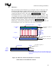
4.2. Inductance:
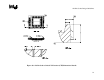
The bottom fixture for the inductance is a ground plane on the secondary side of the
motherboard with all pins grounded. The component side of the socket PCB does
not contain a plane. The top fixture shown is for the package test fixture, which
contains pins that will connect to the socket. Figure 14 presents the inductance
measurement fixture cross-section. The first figure shows the entire assembly. The
second figure shows the assembly without the socket; the socket-seating plane of the
package is directly mounted to the component side of the socket PCB. This is used
to calibrate out the fixture contribution. The materials for the fixture must match the
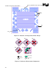
materials used in the package. Figure 16 presents the inductance measurement
methodology. Note the probe pad features exist on the topside of the top fixture, and
the shorting plane exists only on the bottom side of the bottom fixture.
Figure 14: Inductance Measurement Fixture Cross-Section.
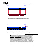
Solder must be formed full and consistent.
Short all L
p
ins
(
usin
g
a solid
p
lane
)
Socket
Top Fixture
(TF)
Bottom Fixture
(BF)
40 mils
probing pads surface
Pins resemble
package or
package type.
Punch through
pins OK
No plane on this layer
Full plane on this layer
No features or plane on
this layer
Short all L
p
ins
(
usin
g
a solid
p
lane
)
Top
Fixture
Bottom
Fixture
40 mils
probing pads
Pins should punch through the motherboard all the way
to the shoulder of the pin. This is the portion that will be
calibrated
No features or plane on
this layer