
Intel Pentium 4 Processor Extreme Edition on 0.13 Micron Process in the 775-Land Package Datasheet


Datasheet 19
Electrical Specifications
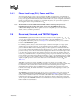
Table 2-2. FSB Signal Groups
Signal Group Type Signals
1
NOTES:
1. Refer to Section 4.2 for signal descriptions.
GTL+ Common Clock Input Synchronous to BCLK[1:0] BPRI#, DEFER#, RESET#, RS[2:0]#, RSP#, TRDY#
GTL+ Common Clock I/O Synchronous to BCLK[1:0]
AP[1:0]#, ADS#, BINIT#, BNR#, BPM[5:0]#, BR0#, DBSY#,
DP[3:0]#, DRDY#, HIT#, HITM#, LOCK#, MCERR#
GTL+ Source Synchronous
I/O
Synchronous to assoc. strobe
Signals Associated Strobe
REQ[4:0]#, A[16:3]#
2
, ADSTB0#
A[35:17]#
2
ADSTB1#
D[15:0]#, DBI0# DSTBP0#, DSTBN0#
D[31:16]#, DBI1# DSTBP1#, DSTBN1#
D[47:32]#, DBI2# DSTBP2#, DSTBN2#
D[63:48]#, DBI3# DSTBP3#, DSTBN3#
2. The value of these signals during the active-to-inactive edge of RESET# defines the processor configuration options. See
Section 6.1 for details.
GTL+ Strobes Synchronous to BCLK[1:0] ADSTB[1:0]#, DSTBP[3:0]#, DSTBN[3:0]#
GTL+Asynchronous Input
A20M#, IGNNE#, INIT#, LINT0/INTR, LINT1/NMI, SMI#, SLP#,
STPCLK#
GTL+Asynchronous Output FERR#/PBE#, IERR#, THERMTRIP#
GTL+ Asynchronous Input/
Output
PROCHOT#
TAP Input Synchronous to TCK TCK, TDI, TMS, TRST#
TAP Output Synchronous to TCK TDO
FSB Clock Clock BCLK[1:0], ITP_CLK[1:0]
3
3. In processor systems where there is no debug port implemented on the system board, these signals are used to support a
debug port interposer. In systems with the debug port implemented on the system board, these signals are no connects.
Power/Other
VCC, VTT, VCCA, VCCIOPLL, VID[5:0], VSS, VSSA,
GTLREF0, COMP[1:0], RESERVED, TESTHI[12:0], THERMDA,
THERMDC, VCC_SENSE, VSS_SENSE, BSEL[2:0],
SKTOCC#, DBR#
3
, VTTPWRGD
4
, PWRGOOD, VTT_SEL,
LL_ID[1:0], GTLREF_SEL, VTT_OUT_LEFT, VTT_OUT_RIGHT
4. VTTPWRGD is not a feature of the Pentium 4 processor Extreme Edition in the 775-land package. This pin is included here for
compatible processors. VTTPWRGD is required for compatibility with Voltage Regulator Down (VRD) 10.1 Design Guide
standards.