
Intel Pentium 4 Processor on 90 nm Process


Datasheet 61
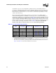
Pin List and Signal Description
§
VCCIOPLL Input
VCCIOPLL
provides isolated power for internal processor FSB PLLs. Follow the
guidelines for VCCA, and refer to the Intel
®
865G/865GV/865PE/865P Chipset
Platform Design Guide for complete implementation details.
VCC_SENSE Output
VCC_SENSE is an isolated low impedance connection to processor core power
(V
CC
). It can be used to sense or measure voltage near the silicon with little
noise.
VCCVID Input
1.2 V is required to be supplied to the VCCVID pin if the platform is going to
support the processor. Refer to the Intel
®
865G/865GV/865PE/865P Chipset
Platform Design Guide for more information.
VCCVIDLB Input
1.2 V is required to be supplied to the VCCVIDLB pin if the platform is going to
support the processor. Refer to the Intel
®
865G/865GV/865PE/865P Chipset
Platform Design Guide for more information.
VID[5:0] Output
VID[5:0] (Voltage ID) pins are used to support automatic selection of power
supply voltages (V
CC
). These are open drain signals that are driven by the
processor and must be pulled up to 3.3 V with 1 kΩ 5% resistors. The voltage
supply for these pins must be valid before the voltage regulator (VR) can supply
V
CC
to the processor. Conversely, the VR output must be disabled until the
voltage supply for the VID pins becomes valid. The VID pins are needed to
support the processor voltage specification variations. See Table 3 for definitions
of these pins. The VR must supply the voltage that is requested by the pins, or
disable itself.
VIDPWRGD Input
The processor requires this input to determine that the V
CCVID
and V
CCVIDLB
voltages are stable and within specification.
VSS Input
VSS are the ground pins for the processor and should be connected to the
system ground plane.
VSSA Input VSSA is the isolated ground for internal PLLs.
VSS_SENSE Output
VSS_SENSE is an isolated low impedance connection to processor core V
SS
. It
can be used to sense or measure ground near the silicon with little noise.
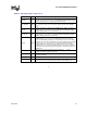
Table 25. Signal Description (Page 8 of 8)
Name Type Description