
Intel Pentium 4 Processor CK00 Clock Synthesizer/Driver Design Guidelines


CK00 Clock Synthesizer/Driver Design Guidelines
Page 10
Where R
Ref
is the external reference resistor and 1.1V was chosen for the reference voltage,
according to the following reasoning:
1) The voltage is close to the voltage that will be present at the final output of the buffer
when generating interesting values of Voh (ie. 0.71V). Thus, the reference voltage
was chosen close to this value to provide an environment better for current mirror
matching.
2) 1.1V is derivable with a clean integer ratio suitable for an accurate internal voltage
divider.
3) 1.1V dictates resistor values of R
Ref
that are available as standard quantities for the
currents of interest.
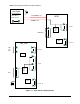
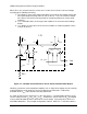
Figure 2.2 – Example Current Reference Circuit Shown with One Buffer Output
Obviously, parameters of the operational amplifier such as input offset voltage must be carefully
understood by the circuit designer to ensure predicted current behavior. Furthermore,
oscillation at the V
Mirror
node could be extremely detrimental.
As shown elsewhere in this document, I
Out
does not equal I
Ref
. Programmable variations of the
current scaling are from I
Out
=4*I
Ref
to I
Out
=7*I
Ref
. Furthermore, chosen values of R
Ref
are allowed
to vary, which will allow for further control of the current output. Interesting values of R
Ref
are
from 200 to 500 Ohms. The principal configuration, however, will be R
Ref
= 475 Ohms with the
I
Out
3.3V
2R
R
~1.1V
R
Ref
I
Ref
C
1
Out
Out
Out_predrv
M
Iref
M
Dum
M
OutB
M
Out
M
Mir
V
Mirror