
Intel Pentium 4 Processor CK00 Clock Synthesizer/Driver Design Guidelines

CK00 Clock Synthesizer/Driver Design Guidelines
Page 11
scale factors set to either I
Out
= 5*I
Ref
or I
Out
= 6*I
Ref
. As shown in Section 8.2, R
Ref
=475
corresponds to an I
Ref
of 2.32mA.
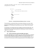
Figure 2.3 – Conventional Current Reference Circuit –
not used
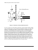
The transistor M
Dum
was included in Figure 2.2 to imitate the drop across one of the switch
transistors at the output (M
Out
or M
OutB
in Figure 2.2). Thus, the voltage environment seen by
MI
Ref
in Figure 2.2 is intended to be similar to M
Mir
, which creates superior current matching
potential.
The capacitor C
1
was included in Figure 2.2 to stabilize the critical current mirror node. Note
that the capacitor C
1
was drawn to 3.3V rather than to ground. This was done to prevent
introducing noise from ground, which would not be correlated to the noise present on the 3.3V
supply of the current mirrors.
2.2 System Implementation
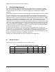
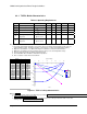
2.2.1 Source termination of differential HCSL type outputs
For systems implementing source termination, it has been discovered that there are significant
benefits gained by adding series resistors in addition to the shunt source termination resistors.
The series resistors along with the termination resistors are illustrated in Figure 2.4. The
benefit is gained due to the extra isolation of the on-die and on-package capacitance from the
line and forces reflected signals to terminate properly through the shunt termination resistors.
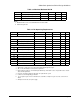
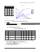
I
Ref
R
Ref
Vdd ~ 3.3V
+
-
Vdiode ~ 0.5V to 1.0V
I
Ref
= [Vdd - Vdiode] / Rr
Vdiode uncertainty would contribute large inaccuracy