
Intel Pentium 4 Processor CK00 Clock Synthesizer/Driver Design Guidelines

CK00 Clock Synthesizer/Driver Design Guidelines
Page 13
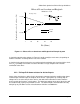
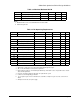
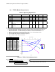
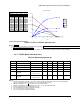
Figure 2.5 – Effect of Rs on Overshoot and Ringback for Example System
It should be noted that the voltages in Figure 2.5 could actually be much worse, depending on
how the reflections are damped in the rest of the network.
It should also be noted also that for cases with matched termination at the load end of the clock
trace, R
S
is probably not needed since there will not be a large component of reflection
terminated at the driver.
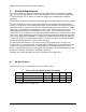
2.2.2 Pull-ups/Pull-down resistors for latched inputs
Some of the clock devices defined in this document incorporate latched or multi-function inputs.
Latched inputs are both inputs and outputs of the device. Upon power-up a voltage high or
voltage low is sensed at the pin of the device, after which the information is latched into the
device and the pin becomes a clock output. The initial input voltage at the pin of the device will
be established by a pull-up or pull-down resistor. The latched inputs should function correctly
with pull-up or pull-down resistors valued between 15kOhms and 500Ohms.
Rs (Ohms)
0
30
1
10
20
40
+ 0.1V
- 0.13V
Ringback and Overshoot (V relative to Voh)
Vovst
Vrbk
Effect of Rs on Overshoot and Ringback
Relative to Voh
Vovst
Vrbk
Example Only