
Intel Pentium 4 Processor CK00 Clock Synthesizer/Driver Design Guidelines

CK00 Clock Synthesizer/Driver Design Guidelines
Page 14
3. Electrical Requirements
This section details the electrical parameters for the differential host clock buffers, multiple
types of 3.3V clock output buffers, and a 5.0V-compatible 3.3V PCI clock driver output buffer.
The different types of 3.3V drivers are needed to compensate for different board layout
topologies.
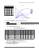
Due to voltage and timing constraints, low-voltage differential swing outputs have been defined.
The clock driver for all clocks must generate monotonic edges through the input threshold
regions as specified for each signaling environment. Many conditions exist in the design of the
clock driver and the system that can affect the monotonic operation of the clock driver. Power
supply noise, pin inductance and capacitance, ratio of clock signals to Vddq and Vss pins, and
routing topology will affect the monotonicity of these clocks. The electrical requirements
outlined here ensure components connect directly together without any external buffers or other
"glue" logic. Series terminating resistors may be required to keep noise within limits on strong
drivers under lightly loaded conditions. Components should be designed to operate within the
"commercial" range of environmental parameters. However, this does not preclude the option
of other operating environments at the vendor's discretion.
The differential clock outputs are specified in terms of their output current accuracy and
transition rate over a range of loads. A default set of signaling criteria is presented along with
ranges for user programmability of the swing amplitude. The driver configuration of these
buffers is strongly dependent on system layout and termination. System information including
layout and termination information is contained in Section 5.
Examples of possible clock driver designs are contained in the appendices.
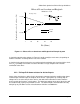
3.1 DC Specifications
DC parameters must be sustainable under steady state (DC) conditions.
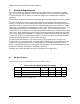
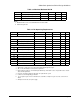
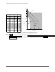
Table 3.1 Absolute Maximum DC Power Supply
Symbol Parameter Min. Max. Units Notes
V
DD3
3.3V Core Supply Voltage -0.5 4.6 V
V
DDQ3
3.3V I/O Supply Voltage -0.5 4.6 V
Ts Storage Temperature -65 150
°
C2
Note: Max Vih not to exceed Vdd3 +0.7V