
Intel Pentium 4 Processor CK00 Clock Synthesizer/Driver Design Guidelines

CK00 Clock Synthesizer/Driver Design Guidelines
Page 15
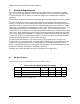
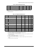
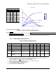
Table 3.2 Absolute Maximum DC I/O
Symbol Parameter Min. Max. Units Notes
V
ih3
3.3V Input High Voltage -0.5 4.6 V 1
V
il3
3.3V Input Low Voltage
−
0.5 V
ESD prot. Input ESD protection 2000 V 2
Notes:
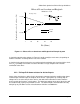
1. Maximum Vih is not to exceed maximum 0.7V above VDD.
2. Human body model.
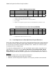
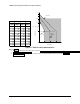
Table 3.3 DC Operating Requirements
Symbol Parameter Condition Min Max Units Notes
V
DD3
3.3V Supply Voltage 3.3V
±
5% 3.135 3.465 V 4
V
ih3
3.3V Input High Voltage VDD3 2.0 V
DD
+0.3 V 7
V
il3
3.3V Input Low Voltage V
SS
-0.3 0.8 V 7
I
il
Input Leakage Current 0 < V
in
< V
DDQ3
-5 +5
µ
A3, 7
V
oh3
3.3V Output High Voltage Ioh = -1 mA 2.4 V 1
V
ol3
3.3V Output Low Voltage Iol = 1 mA 0.4 V 1
V
poh
PCI Bus Output High Voltage Ioh = -1 mA 2.4 V 1
V
pol
PCI Bus Output Low Voltage Iol = 1 mA 0.55 V 1, 5
C
in
Input Pin Capacitance 5 pF 2
C
xtal
Xtal Pin Capacitance 13.5 22.5 pF 6
Ta Ambient Temperature No Airflow 0 70
°
C
Notes:
1. Signal edge is required to be monotonic when transitioning through this region.
2. This is a recommendation, not an absolute requirement.
3. Input Leakage Current does not include inputs with Pull-Up or Pull-down resistors. Inputs with resistors should
state current requirements.
4. No power sequencing is implied or allowed to be required in the system.
5. Conforms to 5V PCI Signaling specification.
6. As seen by the crystal. Device is intended to be used with a 17-20pF AT crystal. See next section for more
details.
7. All inputs referenced to 3.3V power supply.