
Intel Pentium 4 Processor CK00 Clock Synthesizer/Driver Design Guidelines

CK00 Clock Synthesizer/Driver Design Guidelines
Page 16
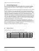
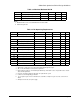
Table 3.3 Maximum Current Draw
Part Parameter Min. Max. Units Notes
CKx_SKS Current from 3.3V supply N/A 250 mA 1,2,3,4
CKx_WBY Current from 3.3V supply N/A 200 mA 1,2,3,4
CKFF Current from 3.3V supply N/A 350 mA 1,4
Notes:
1. Conditions: Max Power supply (3.465V), all active
2. Configured with 475 Ohm current reference resistor at Iout=6*Iref
3. Host = 133MHz
4. Suppliers are encouraged to design for much lower current draw then the specifications shown.
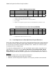
Table 3.4 Maximum Current Draw During PWRDWN#
Part Parameter Min. Max. Units Notes
CKx_SKS Current from 3.3V supply N/A 60 mA 1
CKx_WBY Current from 3.3V supply N/A 80 mA 1
CKFF Current from 3.3V supply N/A 0.3 mA
Notes:
1. Configured with 475 Ohm current reference resistor
3.1.1 Load Capacitance As Seen By External Crystal Reference
Some earlier clock definitions do not specify a target load capacitance for the clock synthesizer
as seen by the crystal. Most of the clock designs targeted 12-13 pF due to historical reasons,
but, few designs specified the variation in their data sheets. However, the common crystals
used today are in the 17-20 pF range.
To reduce the ambiguity with this issue, this specification requires that the clock driver load
capacitance (as seen by the crystal,
not the capacitance of the individual XTAL_IN and
XTAL_OUT pins
)
be targeted
at 18pF +/- 25%.
This specification includes the clock driver
component only and does not include any capacitance associated with board vias and traces.
Doing this:
•
Directs all designs to the same target load capacitance.
•
Requires testing/guarantee by design of the variation.
•
Eliminates external compensation capacitors if the frequency variation can be tolerated.