
Intel Pentium 4 Processor CK00 Clock Synthesizer/Driver Design Guidelines

CK00 Clock Synthesizer/Driver Design Guidelines
Page 17
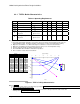
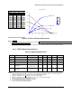
3.2 Buffer Specifications:
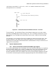
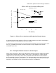
The V/I curves, and Trise/Tfall specifications are targeted at achieving acceptable switching
behavior under the lumped load conditions as described in Section 4 of this specification. Pull-
up and pull-down sides for each of the buffers have separate V/I curves, which are provided, in
the following sections. The DC drive curve specifies steady state conditions that must be
maintained, but does not indicate real output drive strength.
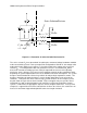
AC parameters must be guaranteed under transient switching (AC) conditions. The sign on all
current parameters (direction of current flow) is referenced to a ground inside the component;
i.e. positive currents flow into the component while negative currents flow out of the component.
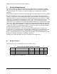
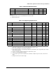
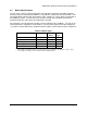
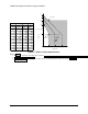
Table 3.4 Buffer Types
Buffer Name VCC Range (V) Impedance
(Ohms)
Buffer
Type
48MHz, REF 3.135 - 3.465 20 - 60 Type 3
PCI, 3V66 3.135 - 3.465 12 - 55 Type 5
MRef, Mref_b 3.135 - 3.465 12 - 55 Type 5
Host/Host_bar Type X1
14seed, 66seed 3.135 - 3.465 12 - 55 Type 5
1. CK00 single ended buffer types are a subset of previous clock driver specifications. Type 1, Type
2,and Type 4 buffer types are not required for this implementation.