
Intel Pentium 4 Processor CK00 Clock Synthesizer/Driver Design Guidelines

CK00 Clock Synthesizer/Driver Design Guidelines
Page 18
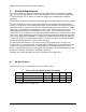
3.2.1 TYPE 3: Buffer Characteristics
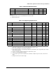
Table 3.5 Operating Requirements
Symbol Parameter Condition Min Typ Max Units Notes
I
ohmin
Pull-Up Current Vout = 1.0 V -29 mA 1
I
ohmax
Pull-Up Current V
out
= 3.135 V -23 mA 1
I
olmin
Pull-Down Current V
out
= 1.95 V 29 mA 1
I
olmax
Pull-Down Current V
out
= 0.4 V 27 mA 1
t
rh
3.3V Type 3 Output Rise
Edge Rate
3.3V
±
5%
@ 0.4V – 2.4 V
0.5 2.0 V/nS 2
t
fh
3.3V Type 3 Output Fall
Edge Rate
3.3V
±
5%
@ 2.4V – 0.4 V
0.5 2.0 V/nS 2
Notes:
1. Intended to approximate impedance curve below. Device should be checked against entire curve for
characterization testing. Production testing is expected to be a subset of characterization testing.
2. Output rise and fall time. See Waveform Figure for calculation / measurement information.
3. Output rise and fall time must be guaranteed across VCC, process and temperature range.
4. Receiver logic thresholds are Vil=0.8 and Vih=2.0 Volts.
5. Ron 20-60 Ohm with a 40 Ohm nominal driver impedance.
6. Ron = Vout/Ioh, Vout/Iol measured at VCC/2.
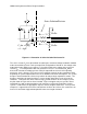
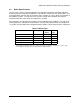
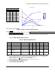
Pull-Up
Voltage I (mA) I (mA) I (mA)
(V) min typ max
0 -29 -46 -99
1 -29 -46 -99
1.4-27-44-94
1.5-27-43-92
1.65 -25 -41 -89
1.8-24-39-85
2 -22 -36 -79
2.4-16-28-63
2.6-12-22-53
3.135 0 -6 -23
3.3 0 -12
3.465 0
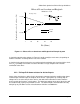
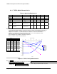
Type3 Pull-Up
-120
-100
-80
-60
-40
-20
0
0 0.5 1 1.5 2 2.5 3 3.5
Vout
IOH
30
50
90
min
typ
max
Figure 3.1 TYPE 3: Pull-Up Characteristics
Notes
(Figure 3.1)
:
1. Must meet the temperature and voltage range specified in
2. Table 3.3 DC Operating Requirements
3. This drawing is not to scale. Comparisons should be made to the data provided in the table next to this
drawing and to Table 3.5 Operating Requirements. .