
Intel Pentium 4 Processor CK00 Clock Synthesizer/Driver Design Guidelines

CK00 Clock Synthesizer/Driver Design Guidelines
Page 21
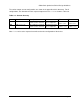
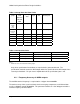
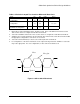
Pull-Down
Voltage I (mA) I(mA) I (mA)
(V) min typ max
0000
0.4 9.4 18 38
0.65 14 30 64
0.85 17.7 38 84
1 20 43 100
1.4 26.5 53 139
1.5 28 55 148
1.65 29 56 163
1.8 30 57 175
1.95 30 58 178
3.135 31 59 187
3.6 32 59 188
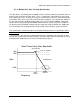
DC Drive Point
AC Drive Point
Test Point
Current (mA)
V
DD
1.8
30
175
0
0.3
Voltage (V)
0
Typical
Conditions
57
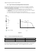
Figure 3.4 TYPE 5: PCI Clock Output Buffer Pull-Down Characteristics
Notes
(Figure 3.4)
:
1. Must meet the temperature and voltage range specified in
2. Table 3.3 DC Operating Requirements
3. This drawing is not to scale. Comparisons should be made to the data provided in the table next to it and to Table 3.6:
Operating Requirements