
Intel Pentium 4 Processor CK00 Clock Synthesizer/Driver Design Guidelines

CK00 Clock Synthesizer/Driver Design Guidelines
Page 22
3.2.3 Type X1 Current-mode Output Buffer Characteristics
The current-mode output buffer details and current reference circuit details are contained
elsewhere in this document. For the purposes of this section, the following parameters are
used to specify output buffer characteristics:
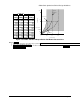
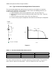
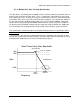
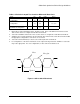
1) Output impedance of the current mode buffer circuit – Ro (See Figure 3.5)
2) Minimum and maximum required voltage operation range of the circuit – Vop (See
Figure 3.1)
3) Series resistance in the buffer circuit – Ros (See Figure 3.5)
4) Current accuracy at given configuration into nominal test load for given configuration
Ro
Ros
Iout
Vdd3
(3.3V +/- 5%)
Vout = 1.2V max
Iout
Slope ~ 1 / Ro
Vout
1.2V
0V
Figure 3.5
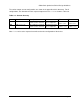
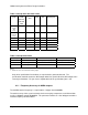
Table 3.7 - Host Clock (HCSL) Buffer Characteristics
Minimum Maximum
Ro 3000 Ohms (recommended) N/A
Ros unspecified unspecified
Vout N/A 1.2V
The reader should note that Iout is selectable depending on implementation. The parameters
above, however, apply to all configurations. Vout is the voltage at the pin of the device.