
Intel Pentium 4 Processor CK00 Clock Synthesizer/Driver Design Guidelines

CK00 Clock Synthesizer/Driver Design Guidelines
Page 24
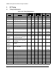
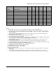
4. AC Timing
4.1 Timing Requirements
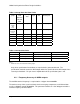
Table 4.1 AC Timing Requirements
133 MHz Host 100 MHz Host
Symbol Parameter Min Max Min Max Units Notes
TPeriod Host CLK period - average 7.5 7.65 10.0 10.2 nS 11, 14
AbsMinPeriod Absolute minimum Host CLK Period 7.35 N/A 9.85 N/A nS 11, 14
Ioh
(Voh)
Output Current
(Voltage at given load)
12.9
(0.65)
14.9
(0.74)
12.9
(0.65)
14.9
(0.74)
mA
(V)
11, 13, 17
Vol Vss =
0.0
0.05 Vss =
0.0
0.05 V 11
Vcrossover 45%
Voh
55%
Voh
45%
Voh
55%
Voh
V 11, 14
TRISE Host/CPU CLK rise time 175 700 175 700 pS 11, 15
TFALL Host/CPU CLK fall time 175 700 175 700 pS 11, 15
Rise/Fall
Matching
Rise time and fall time matching 20% 20% 11, 16
Overshoot Voh +
0.2V
Voh +
0.2V
11, 16
Undershoot – 0.2V – 0.2V 11
Tskew
(One chip
partition)
Pair to Pair skew for one chip partition
for
CKx_SKS, CKx_RGR
150 150 pS 11, 14
Tskew
(Two chip
partition)
Pair to Pair skew for two chip partition
for
CKx_WBY
100 100 pS
11, 14
Tccjitter
(One chip
partition)
Cycle to Cycle jitter for
CKx_SKS,
CKx_RGR
200 200 pS 11, 12, 14
Tccjitter
(Two chip
partition)
Cycle to Cycle jitter for two chip
partition for
CKx_WBY
150 150 pS 11, 12, 14
Duty Cycle 45% 55% 45% 55% 11, 14
TPeriod Mref, Mref_b CLK period 15.0 15.3 20.0 20.4 nS 2, 9
THIGH MRef, Mref_b CLK high time 5.25 N/A 7.5 N/A nS 5, 10
TLOW MRef, Mref_b CLK low time 5.05 N/A 7.3 N/A nS 6, 10
TRISE MRef, Mref_b CLK rise time 0.4 1.6 0.4 1.6 nS 8
TFALL MRef, Mref_b CLK fall time 0.4 1.6 0.4 1.6 nS 8
TPeriod 3V66 CLK period 15.0 16.0 15.0 15.2 2, 4, 9
THIGH 3V66 CLK high time 5.25 N/A 5.25 N/A 5 ,10