
Intel Pentium 4 Processor CK00 Clock Synthesizer/Driver Design Guidelines

CK00 Clock Synthesizer/Driver Design Guidelines
Page 25
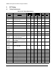
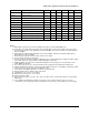
TLOW 3V66 CLK low time 5.05 N/A 5.05 N/A 6 ,10
TRISE 3V66 CLK rise time 0.5 2.0 0.5 2.0 8
TFALL 3V66 CLK fall time 0.5 2.0 0.5 2.0 8
TPeriod PCI CLK period 30.0 N/A 30.0 N/A nS 2, 3, 9
THIGH PCI CLK high time 12.0 N/A 12.0 N/A nS 5 ,10
TLOW PCI CLK low time 12.0 N/A 12.0 N/A nS 6 ,10
TRISE PCI CLK rise time 0.5 2.0 0.5 2.0 nS 8
TFALL PCI CLK fall time 0.5 2.0 0.5 2.0 nS 8
tpZL, tpZH Output enable delay (All outputs) 1.0 10.0 1.0 10.0 nS
tpLZ, tpZH Output disable delay (All outputs) 1.0 10.0 1.0 10.0 nS
tstable All clock Stabilization from power-up 3 3 mS 7
Notes:
1. Output drivers must have monotonic rise/fall times through the specified VOL/VOH levels.
2. Period, jitter, offset and skew measured on rising edge @1.25V for 2.5V clocks and @ 1.5V for 3.3V clocks.
3. The PCI clock is the Host clock divided by four at Host=133MHz. PCI clock is the Host clock divided by three
at Host = 100MHz.
4. 3V66 is internal VCO frequency divided by four for Host=133MHz. 3V66 clock is internal VCO frequency
divided by three for Host=100MHz
5. T
HIGH
is measured at 2.0V for 2.5V outputs, 2.4V for 3.3V outputs.
6. T
LOW
is measured at 0.4V for all outputs.
7. The time specified is measured from when Vddq achieves its nominal operating level (typical condition Vddq =
3.3V) till the frequency output is stable and operating within specification.
8. TRISE and TFALL are measured as a transition through the threshold region Vol = 0.4V and Voh = 2.4V
(1mA) JEDEC Specification.
9. The average period over any 1 uS period of time must be greater than the minimum specified period
10. Calculated at minimum edge-rate (1V/nS) to guarantee 45/55% duty-cycle. Pulsewidth is required to be wider
at faster edge-rate to ensure duty-cycle specification is met.
11. Test load is Rs=33.2Ohms, Rp=49.9. See Section 5, and Table 6.9.
12. Must be guaranteed in a realistic system environment.
13. Configured for Ioh = 6 * Iref. See Section 5.
14.
Measured at crossing points. See section 5.
15.
Measured at 20% to 80%.
16. Determined as a fraction of 2*(Trp – Trn) / (Trp + Trn) where Trp is a rising edge and Trn is an intersecting
falling edge.
17. These minimum and maximum voltages and currents assume a power supply of 3.30V. For system
considerations, the voltages will need to be degraded to account for the +/-5% variation in the 3.3V supply.