
Intel Pentium 4 Processor CK00 Clock Synthesizer/Driver Design Guidelines

CK00 Clock Synthesizer/Driver Design Guidelines
Page 26
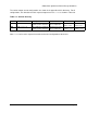
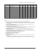
Table 4.2 Group Skew And Jitter Limits
Output
group
Pin-pin
Skew
Or Pair-to-
Pair Skew
MAX
Cycle-Cycle
Jitter
Duty
Cycle
Nom
Vdd
Skew, jitter
measure point
Host
(Single
Pkg
Case)
150 pS 200 pS 45/55 N/A Crossing
Host
(Dual Pkg
Case)
100 pS 150pS 45/55 N/A Crossing
MRef N/A 250 pS 45/55 3.3 V 1.5 V
48MHz N/A 350 pS 45/55 3.3 V 1.5 V
3V66 250 pS 300 pS 45/55 3.3 V 1.5 V
PCI 500 pS 500 pS 45/55 3.3 V 1.5 V
REF N/A 1000 pS 45/55 3.3V 1.5 V
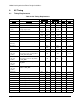
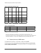
Table 4.3 Group Offset limits
Group Offset Measurement loads (lumped) Measure Points
3V66 to PCI 1.5-3.5 nS 3V66 leads 3V66@30 pF, PCI@30 pF 3V66@1.5 V, PCI@1.5 V
Host to 3V66 No Requirement
Host to PCI No Requirement
Notes:
1. All offsets are to be measured at rising edges
Only offset specifications listed above are required to be guaranteed/tested. The
specification should be treated as ANY output within first specified bank to ANY output of the
second specified bank. Pin-pin skew is implied within offset specification; jitter is not.
4.1.1 Frequency Accuracy of 48MHz outputs
The 48 MHz nominal frequency is required to be +167ppm from 48.00MHz.
The total accuracy of the crystal and clock device over aging, temperature, and Vdd variation
must be ± 500ppm around 48.000MHz. This parameter amounts to +333/-667ppm around the
nominal frequency identified above.