
Intel Pentium 4 Processor CK00 Clock Synthesizer/Driver Design Guidelines

CK00 Clock Synthesizer/Driver Design Guidelines
Page 28
5. Test and Measurement
The tables below provide acceptable lumped load test loads over which the vendor is expected
to test and guarantee all AC parameters for the clock driver. The vendor is encouraged to
provide information on the correlation between lumped load performance and system
performance as an applications exercise to fully describe the operation of the product.
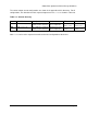
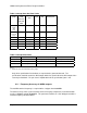
Table 5.1 -- Lumped Capacitive Test Loads for Single Ended Outputs
Clock Min
Load
Max
Load
Units Notes
PCI Clocks (PCLK) 10 30 pF Must meet PCI 2.1 requirements
Mref, Mref_b 10 30 pF 1 device load, possible 2 loads
3V66 10 30 pF 1 device load, possible 2 loads
48 MHz Clock 10 20 pF 1 device load
REF 10 20 pF 1 device load
Notes:
1. Maximum rise/fall times are to be guaranteed at maximum specified load for each type of output buffer.
2. Minimum rise/fall times are to be guaranteed at minimum specified load for each type of output buffer
3. Rise/fall times are specified with pure capacitive load as shown. Testing may be done with an additional 500
ohm resistor in parallel if properly correlated with the capacitive load.
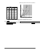
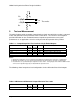
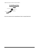
The following shows lumped test load configurations for the differential Host Clock outputs.
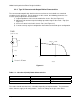
Table 5.2 Minimum and Maximum Lumped Resistive Test Loads
Clock Min
Load
Max
Load
Units Notes
Host Clocks 20 105 Ohms
Rp
Rp
Rs
Rs
Test nodes