
Intel Pentium 4 Processor CK00 Clock Synthesizer/Driver Design Guidelines

CK00 Clock Synthesizer/Driver Design Guidelines
Page 33
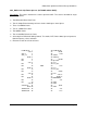
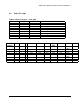
CKx_WBY clock chip (48 SSOP Package and 48 TSSOP):
Description: This is intended as the main clock source in certain multiple-chip clock partitions.
This clock is intended to be used with the FF. The WBY/FF pair is intended to be used in two-
processor, and four-processor platforms.
!
Six Differential Host Clock Pairs
!
Two 3V Single Ended memory reference clocks 180 degrees out of phase
!
One 66MHz reference output
!
One14.318MHz reference output
!
Select logic for Differential Swing Control, Test mode, Hi-Z, Powerdown, Spread spectrum,
limited frequency select, selective clock enable.
!
External resistor for current reference
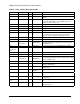
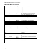
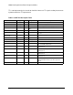
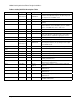
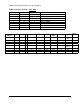
GndR 1 48 3.3R
ref_out 2 47 Gnd
3.3R 3 46 3.3H
Xtal_in 4 45 Host
Xtal_out 5 44 Host_bar
GndR 6 43 GndH
3.3M 7 42 Host
3VMref 8 WBY 41 Host_bar
3VMref_b 9 40 3.3H
GndM 10 39 Host
3.3Core 11 38 Host_bar
3.3Gnd 12 37 GndH
3.3L 13 36 Host
3V66 14 35 Host_bar
GndL 15 34 3.3H
Sel100/133 16 33 Host
MultSel0 17 32 Host_bar
MultSel1 18 31 GndH
3.319 30Host
Gnd 20 29 Host_bar
SelA 21 28 3.3H
SelB 22 27 I Ref
Spread# 23 26 GndI
PWRDWN# 24 25 3.3I