
Intel Pentium 4 Processor CK00 Clock Synthesizer/Driver Design Guidelines
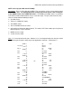

CK00 Clock Synthesizer/Driver Design Guidelines
Page 35
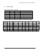
CKFF clock chip (48 SSOP and 48 TSSOP):
Description: This is a slave clock to the WBY. This can also be used as a slave clock to future
variants of the WBY.
For Spread Spectrum Tracking, there must not be a PLL in the path
of the 66MHz clocks or the 33MHz PCI clocks.
The 66MHz and 33MHz clocks are intended
to be buffered and/or divided from the 66_in seed clock input. The pin-out of this device was
chosen to allow down-bondability to 48 pins
!
Six 3V66 Clocks
!
Twelve 3V, 33MHz PCI Clocks
!
Two 48MHz Clocks
!
Two 14.318MHz Reference Clocks
!
Select logic for Differential Swing Control, Test mode, Hi-Z, Power-down, Spread spectrum,
limited frequency select, and other
!
66MHz reference input
!
14.318 reference input
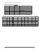
Note: I
2
C is not required for this part. However, if I
2
C is not implemented, then the part should
be a different part number in order to prevent applications confusion. Furthermore, if
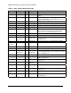
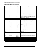
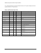
GndN 1 56 3.3R
14.318_in 2 55 Ref
3.3N 3 54 Ref
66_in 4 53 GndR
GndP 5 52 3.3L
PCI 6 51 3V66
PCI 7 50 3V66
3.3P 8 49 GndL
GndP 9 48 GndL
PCI 10 47 3V66
PCI 11 46 3V66
3.3P 12 45 3.3L
GndP 13 FF 44 3.3L
PCI 14 43 3V66
PCI 15 42 3V66
3.3P 16 41 GndL
PCI 17 40 3.3
PCI 18 39 Gnd
GndP 19 38 3.3U
3.3P 20 37 48Mhz
PCI 21 36 48Mhz
PCI 22 35 GndU
GndP 23 34 Sels
PCI 24 33 PWRDWN#
PCI 25 32 3.3S
3.3P 26 31 GndS
Selq 27 30 Sclock
Selr 28 29 Sdata