
Intel Pentium 4 Processor CK00 Clock Synthesizer/Driver Design Guidelines

CK00 Clock Synthesizer/Driver Design Guidelines
Page 36
I
2
C is not implemented, pins 29 and 30 should be immune to I
2
C signals to allow placement on
a platform which has I
2
C implemented.
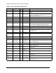
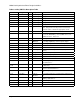
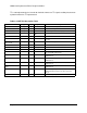
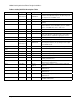
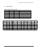
Table 6.3 CKFF Pin Description Table
Pin Type Qty Symbol Description
55,54 3.3V output 2 Ref 14.318MHz 3.3V outputs
51,50,47,46,43,42 3.3V output 6 3V66 66MHz 3.3V outputs
37,36 3.3V output 2 48MHz 48MHz output. See accuracy specifications.
34,28,27 Input 3 SELq, SELr,
SELs
Select Pins
33 Input 1 PWRDWN# Invokes Power-down mode. Active Low.
30,29 Input Sclock, Sdata
I
2
C pins
25,24,22,21,18,17,15,
14,11,10,7,6
3.3V output 12 PCI 3.3V 33MHz outputs
4 Input 1 66_in Input for 3.3V 66MHz reference clock
2 Input 1 14.318_in Input for 14.318MHz reference clock
56,53 Power/Gnd 3.3R,GndR Power and ground pins recommended for REF
clock and Xtal dedicated use
52,49,48,45,44,41 Power/Gnd 3.3L,GndL Power and ground pins recommended for 3V66
dedicated use
38,35 Power/Gnd 3.3U, GndU Power and ground pins recommended for 48MHz
dedicated use
32,31 Power/Gnd 3.3S, GndS Power and ground pins recommended for I^2C
dedicated use
26,23,20,19,16,13,12,
9,8,5
Power/Gnd 3.3P,GndP Power and ground pins recommended for PCI
dedicated use
3,1 Power/Gnd 3.3N, GndN Power and ground pins recommended for
dedicated input circuit use (for 14.318_in and
66_in)
40,39 Power, Gnd 3.3, Gnd Power and ground pins