
Intel Pentium 4 Processor CK00 Clock Synthesizer/Driver Design Guidelines

CK00 Clock Synthesizer/Driver Design Guidelines
Page 46
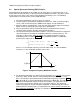
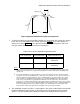
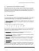
output clocks, is shown in Figure 7, as functions of modulation frequency, modulation
profile, and spread amount. This plot is obtained through PLL behavior simulations
assuming a jitter-free ideal modulated input clock to the PLL. The parameters of the
simulated PLL are:
(VCO gain) * (charge-pump current) = 2800 (Hz/V)(A),
feedback divider
=2,
2
nd
-order filter:
C
1
= 11 pF; C2 = 356 pF; R = 9.75 k
Ω.
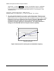
9. This skew should be minimized, as it reduces system timing margins. Different system
implementations have different requirements and PLL characteristics, and may require
tighter or looser skew. It is always true that a lower modulation frequency results in smaller
tracking skew. The skew is proportional to the amount of spreading.
Any implemented
modulation profile must induce less than 110 pS skew with the above PLL
parameters by properly adjusting its spread amount. Sinusoidal modulation is
strongly not recommended
due to its low peak reduction capability.
80
100
120
140
160
180
200
220
30 40 50 60 70 80 90 100
Modulation Frequency [kHz]
Skew [ps]
Linear Modulation (
δ
= 0.6%)
Non-Linear Modulation (
δ
= 0.5%)
Figure 7 Downstream PLL tracking skew and modulation frequency