
Intel Pentium 4 Processor CK00 Clock Synthesizer/Driver Design Guidelines

CK00 Clock Synthesizer/Driver Design Guidelines
Page 49
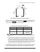
6.7 Defined option for PCI_bankSTOP# functionality
For the SKS and RGR clock devices, an option should be included such that the Spread# pin
would be replaced by a PCI_bankSTOP# pin which will shut off (hold LOW) the top five PCI
clocks (pins 8,9,11,12,14 for the SKS and pins 6,7,9,10,12 for the RGR). The PCI_bankSTOP#
pin should be active LOW. In a system where PCI_bankSTOP# is implemented, spread
spectrum will be defaulted to ON.
6.8 I
2
C Considerations
I
2
C has been chosen as the serial bus interface to control these clock drivers. I
2
C was chosen
to support the JEDEC proposal JC-42.5 168 Pin Unbuffered SDRAM DIMM. All vendors are
required to determine the legal issues associated with the manufacture of I
2
C devices.
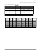
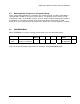
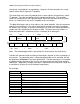
1) Address assignment: Any clock driver in this specification can use the single, 7 bit
address shown below. All devices can use the address if only one master clock driver
is used in a system.
The following address was confirmed by Philips on 09/04/96.
A6 A5 A4 A3 A2 A1 A0 R/W#
1101001 0
Note:
The R/W# bit is used by the I2C controller as a data direction bit. A ‘zero’ indicates a transmission (WRITE)
to the clock device. A ‘one’ indicates a request for data (READ) from the clock driver. Since the definition of the
clock buffer only allows the controller to WRITE data; the R/W# bit of the address will always be seen as a ‘zero.’
Optimal address decoding of this bit is left to the vendor.
2) Slave/Receiver: The clock driver is assumed to require only slave/receiver
functionality. Slave/transmitter functionality is optional.
3) Data Transfer Rate: 100 kbits/s (standard mode) is the base functionality required.
Fast mode (400 kbits/s) functionality is optional.
4) Logic Levels: I
2
C logic levels are based on a percentage of VDD for the controller
and other devices on the bus. Assume all devices are based on a 3.3 Volt supply.
5) Data Byte Format: Byte format is 8 Bits as described in the following appendices.
6) Data Protocol:
To simplify the clock I
2
C interface, the clock driver serial protocol was specified to use
only block writes from the controller. The bytes must be accessed in sequential order
from lowest to highest byte with the ability to stop after any complete byte has been