
Intel Pentium 4 Processor CK00 Clock Synthesizer/Driver Design Guidelines

CK00 Clock Synthesizer/Driver Design Guidelines
Page 51
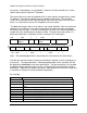
A transfer is considered valid after the acknowledge bit corresponding to the byte count
is read by the controller. The serial controller interface can be simplified by discarding
the information in both the command code and the byte count bytes and simply reading
all the bytes that are sent to the clock driver after being addressed by the controller. It
is expected that the controller will not provide more bytes than the clock driver can
handle. A clock vendor may choose to discard any number of bytes that exceed the
defined byte count.
8) Clock Stretching: The clock device must not hold/stretch the SCLOCK or SDATA
lines low for more than 10 mS. Clock stretching is discouraged and should only be
used as a last resort. Stretching the clock/data lines for longer than this time puts the
device in an error/time-out mode and may not be supported in all platforms. It is
assumed that all data transfers can be completed as specified without the use of
clock/data stretching.
9) General Call: It is assumed that the clock driver will not have to respond to the
“general call.”
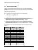
10) Electrical Characteristics: All electrical characteristics must meet the standard
mode specifications found in section 15 of the I
2
C specification.
a) Pull-Up Resistors: Any internal resistor pull-ups on the SDATA and SCLOCK inputs
must be stated in the individual datasheet. The use of internal pull-ups on these pins of
below 100K is discouraged. Assume that the board designer will use a single external
pull-up resistor for each line and that these values are in the 5 - 6K Ohm range.
Assume one I
2
C device per DIMM (serial presence detect), one I
2
C controller, one clock
driver plus one/two more I
2
C devices on the platform for capacitive loading purposes.
b) Input Glitch Filters: Only fast mode I
2
C devices require input glitch filters to suppress
bus noise. The clock driver is specified as a standard mode device and is not required
to support this feature. However, it is considered a good design practice to include the
filters.
11) PWR_DWN#: If a clock driver is placed in PWR_DWN# mode, the SDATA and
SCLK inputs must be Tri-Stated and the device must retain all programming
information. Idd current due to the I
2
C circuitry must be characterized and in the
datasheet.
For specific I
2
C information consult the Philips I
2
C Peripherals Data Handbook ICI2
(1996)