
Intel Pentium 4 Processor CK00 Clock Synthesizer/Driver Design Guidelines
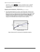

CK00 Clock Synthesizer/Driver Design Guidelines
Page 52
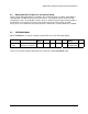
6.9 I
2
C Byte Locations for CKFF
At power up all CKFF outputs should be enabled and active. The Sdata and Sclock inputs
should both have internal pull-up resistors with values above 100K Ohms for complete platform
flexibility.
CKFF Serial Configuration Map
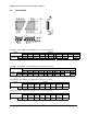
A) The serial bits will be read by the clock driver in the following order:
Byte 0 - Bits 7, 6, 5, 4, 3, 2, 1, 0
Byte 1 - Bits 7, 6, 5, 4, 3, 2, 1, 0
.
Byte N - Bits 7, 6, 5, 4, 3, 2, 1, 0
B) All unused register bits (reserved and N/A) should be designed as don’t care. It is
expected that the controller will force all of these bits to a “0” level.
C) All register bits labeled “Initialize to 0” must be written to zero during initialization.
Failure to do so may result in a higher then normal operating current. The controller
will read back the last written value.
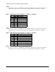
For the purposes of this section, the following labels are used to designate various
outputs.
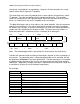
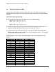
Output Type CKFF Pin Label
PCI 6 PCI0
PCI 7 PCI1
PCI 10 PCI2
PCI 11 PCI3
PCI 14 PCI4
PCI 15 PCI5
PCI 17 PCI6
PCI 18 PCI7
PCI 21 PCI8
PCI 22 PCI9
PCI 24 PCI10
PCI 25 PCI11
48MHz 36 48M0
48MHz 37 48M1
3V66 42 66M0
3V66 43 66M1
3V66 46 66M2
3V66 47 66M3
3V66 50 66M4
3V66 51 66M5
14.318MHz 54 14M0
14.318MHz 55 14M1