
Intel Pentium 4 Processor CK00 Clock Synthesizer/Driver Design Guidelines

CK00 Clock Synthesizer/Driver Design Guidelines
Page 54
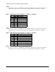
Notes:
3. Inactive means outputs are held LOW and are disabled from switching. These outputs are designed to be
configured at power-on and are not expected to be configured during the normal modes of operation,
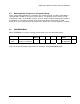
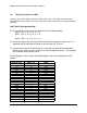
Byte 3 : CKFF Active/Inactive Register (1 = enable, 0 = disable)
Bit Name Description
Bit 7 (Reserved for Intel)
Bit 6 (Reserved for Intel)
Bit 5 (Reserved for Intel)
Bit 4 (Reserved for Intel)
Bit 3 (Reserved for Intel)
Bit 2 (Reserved for Intel)
Bit 1 (Reserved for Intel)
Bit 0 (Reserved for Intel)
Notes:
4. Inactive means outputs are held LOW and are disabled from switching. These outputs are designed to be
configured at power-on and are not expected to be configured during the normal modes of operation,
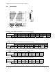
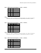
Byte 4 : CKFF Active/Inactive Register (1 = enable, 0 = disable)
Bit Name Description
Bit 7 (Reserved for clock supplier)
Bit 6 (Reserved for clock supplier)
Bit 5 (Reserved for clock supplier)
Bit 4 (Reserved for clock supplier)
Bit 3 (Reserved for clock supplier)
Bit 2 (Reserved for clock supplier)
Bit 1 (Reserved for clock supplier)
Bit 0 (Reserved for clock supplier)
Notes:
5. Inactive means outputs are held LOW and are disabled from switching. These outputs are designed to be
configured at power-on and are not expected to be configured during the normal modes of operation,