
Intel Pentium 4 Processor Extreme Edition on 0.13 Micron Process in the 775-Land Package Datasheet

18 Datasheet
Electrical Specifications
The TESTHI signals may use individual pull-up resistors or be grouped together as detailed below.
A matched resistor must be used for each group:
• TESTHI0 – cannot be grouped with other TESTHI signals
• TESTHI1 – cannot be grouped with other TESTHI signals
• TESTHI[7:2]
• TESTHI8 – cannot be grouped with other TESTHI signals
• TESTHI9 – cannot be grouped with other TESTHI signals
• TESTHI10 – cannot be grouped with other TESTHI signals
• TESTHI11 – cannot be grouped with other TESTHI signals
• TESTHI12 – cannot be grouped with other TESTHI signals
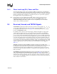
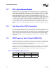
2.6 FSB Signal Groups
The FSB signals have been combined into groups by buffer type. GTL+ input signals have
differential input buffers that use GTLREF0 as a reference level. In this document, the term “GTL+
Input” refers to the GTL+ input group as well as the GTL+ I/O group when receiving. Similarly,
“GTL+ Output” refers to the GTL+ output group as well as the GTL+ I/O group when driving.
With the implementation of a source synchronous data bus comes the need to specify two sets of
timing parameters. One set is for common clock signals which are dependent upon the rising edge
of BCLK0 (ADS#, HIT#, HITM#, etc.) and the second set is for the source synchronous signals
that are relative to their respective strobe lines (data and address) as well as the rising edge of
BCLK0. Asychronous signals are still present (A20M#, IGNNE#, etc.) and can become active at
any time during the clock cycle. Table 2-2 identifies which signals are common clock, source
synchronous, and asynchronous.