
Intel Pentium 4 Processor Extreme Edition on 0.13 Micron Process in the 775-Land Package Datasheet

22 Datasheet
Electrical Specifications
2.11 Processor DC Specifications
The processor DC specifications in this section are defined at the processor core silicon and
not at the package lands unless noted otherwise. See Chapter 4 for the signal definitions and
signal assignments. Most of the signals on the processor FSB are in the GTL+ signal group. The
DC specifications for these signals are listed in Table 2-7.
Previously, legacy signals and Test Access Port (TAP) signals to the processor used low-voltage
CMOS buffer types. However, these interfaces now follow DC specifications similar to GTL+. The
DC specifications for these signal groups are listed in Table 2-8 and Table 2-9.
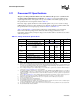
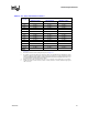
Table 2-5 through Table 2-11 list the DC specifications for the Pentium 4 processor Extreme
Edition in the 775-land package and are valid only while meeting specifications for case
temperature, clock frequency, and input voltages. Care should be taken to read all notes associated
with each parameter.
Table 2-5. Voltage and Current Specifications
Symbol Parameter Min Typ Max Unit Notes
1
NOTES:
1. Unless otherwise noted, all specifications in this table are based on estimates and simulations or empirical data. These spec-
ifications will be updated with characterized data from silicon measurements at a later date.
VID range VID 1.525 — 1.600 V
2
2. Each processor is programmed with a maximum valid voltage identification value (VID), which is set at manufacturing and
can not be altered. Individual maximum VID values are calibrated during manufacturing such that two processors at the
same frequency may have different settings within the VID range.
V
CC
V
CC
for 775_VR_CONFIG_04B See Table 2-6 and Figure 2-1.V
3, 4, 5, 6
3. These voltages are targets only. A variable voltage source should exist on systems in the event that a different voltage is
required. See Section 2.4 and Table 2-1 for more information.
4. The voltage specification requirements are measured across VCC_SENSE and VSS_SENSE lands at the socket with a
100 MHz bandwidth oscilloscope, 1.5 pF maximum probe capacitance, and 1 MΩ minimum impedance. The maximum
length of ground wire on the probe should be less than 5 mm. Ensure external noise from the system is not coupled into the
oscilloscope probe.
5. Refer to Table 2-6 and Figure 2-1 for the minimum, typical, and maximum V
CC
allowed for a given current. The processor
should not be subjected to any V
CC
and I
CC
combination wherein V
CC
exceeds V
CC_max
for a given current.
6. Adherence to this loadline specification for the processor is required to ensure reliable processor operation.
I
CC
I
CC
for processor with multiple VID:
3.40 GHz
3.46 GHz
— — 83.9
84.8
A
6,
7
7. I
CC_max
is specified at V
CC_max
.
I
SGNT
I
SLP
I
CC
Stop-Grant — — 40 A
8, 9
8. The current specified is also for AutoHALT State.
9. Icc Stop-Grant and Icc Sleep are specified at V
CC_max
.
I
TCC
I
CC
TCC active — — I
CC
A
10
10. The maximum instantaneous current the processor will draw while the thermal control circuit is active as indicated by the
assertion of PROCHOT# is the same as the maximum Icc for the processor.
I
CC PLL
I
CC
for PLL lands — — 60 mA —
V
TT
Miscellaneous voltage supply 1.14 1.20 1.26 V
11,
12
11. V
TT
must be provided via a separate voltage source and not connected to V
CC
. This specification is measured at the land.
12. Baseboard bandwidth is limited to 20 MHz.
VTT_OUT I
CC
DC current that may be drawn from
VTT_OUT per pin
— — 580 mA —