
Intel Pentium 4 Processor Extreme Edition on 0.13 Micron Process in the 775-Land Package Datasheet

Datasheet 25
Electrical Specifications
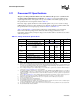
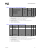
Table 2-8. Asynchronous GTL+ Signal Group DC Specifications
Symbol Parameter Min Max Unit Notes
1
NOTES:
1. Unless otherwise noted, all specifications in this table apply to all processor frequencies and voltages.
V
IH
Input High Voltage, Asynch GTL+ 1.10*GTLREF0 V
CC
V
2,3,4
2. V
IH
and V
OH
may experience excursions above V
CC
. However, input signal drivers must comply with the sig-
nal quality specifications.
3. The V
CC
referred to in these specifications refers to instantaneous V
CC
.
4. This specification applies to the asynchronous GTL+ signal group.
V
IL
Input Low Voltage, Asynch. GTL+ 0 0.9*GTLREF0 V
4
V
OH
Output High Voltage N/A V
CC
V
2,3,5
5. All outputs are open-drain.
I
OL
Output Low Current N/A 50 mA
6
6. The maximum output current is based on maximum current handling capability of the buffer.
I
HI
Land Leakage High N/A 100 µA
7
7. Leakage to V
SS
with land held at V
CC
.
I
LO
Land Leakage Low N/A 500 µA
8
8. Leakage to V
CC
with land held at 300 mV.
R
ON
Buffer On Resistance, Asynch GTL+ 8.4 13.2 Ω
4
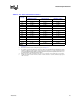
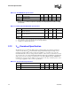
Table 2-9. PWRGOOD and TAP Signal Group DC Specifications
Symbol Parameter Min Max Unit Notes
1
NOTES:
1. Unless otherwise noted, all specifications in this table apply to all processor frequencies and voltages.
V
HYS
Input Hysteresis 200 300 mV
2
2. V
HYS
represents the amount of hysteresis, nominally centered about 1/2 V
CC
for all TAP inputs.
V
T+
Input Low-to-High
Threshold Voltage
1/2*(V
CC
+V
HYS_MIN
)1/2*(V
CC
+V
HYS_MAX
)V
3
3. The V
CC
referred to in these specifications refers to instantaneous V
CC
.
V
T-
Input High-to-Low
Threshold Voltage
1/2*(V
CC
–V
HYS_MAX
)1/2*(V
CC
–V
HYS_MIN
)V
3
V
OH
Output High Voltage N/A V
CC
V
3,4,5
4. All outputs are open-drain.
5. The TAP signal group must comply with the signal quality specifications. Contact your Intel representative
for further documentation.
I
OL
Output Low Current N/A 40 mA
6
6. The maximum output current is based on maximum current handling capability of the buffer.
I
HI
Land Leakage High N/A 100 µA
7
7. Leakage to V
SS
with land held at V
CC
.
I
LO
Land Leakage Low N/A 500 µA
8
8. Leakage to V
CC
with land held at 300 mV.
R
ON
Buffer On Resistance 8.75 13.75 Ω