
Intel Pentium 4 Processor Extreme Edition on 0.13 Micron Process in the 775-Land Package Datasheet

63 Datasheet
Land Listing and Signal Descriptions
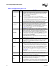
DRDY#
Input/
Output
DRDY# (Data Ready) is asserted by the data driver on each data transfer,
indicating valid data on the data bus. In a multi-common clock data transfer,
DRDY# may be de-asserted to insert idle clocks. This signal must connect the
appropriate pins/lands of all processor FSB agents.
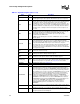
DSTBN[3:0]#
Input/
Output
DSTBN[3:0]# are the data strobes used to latch in D[63:0]#.
DSTBP[3:0]#
Input/
Output
DSTBP[3:0]# are the data strobes used to latch in D[63:0]#.
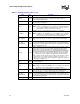
FC[14:0] Other
Future compatible lands are reserved to be used with future or compatible
processors. Contact your Intel representative for further documentation.
FC16 Other
Future compatible lands are reserved to be used with future or compatible
processors. Contact your Intel representative for further documentation.
FERR#/PBE# Output
FERR#/PBE# (floating point error/pending break event) is a multiplexed signal
and its meaning is qualified by STPCLK#. When STPCLK# is not asserted,
FERR#/PBE# indicates a floating-point error and will be asserted when the
processor detects an unmasked floating-point error. When STPCLK# is not
asserted, FERR#/PBE# is similar to the ERROR# signal on the Intel 387
coprocessor, and is included for compatibility with systems using MS-DOS*-
type floating-point error reporting. When STPCLK# is asserted, an assertion of
FERR#/PBE# indicates that the processor has a pending break event waiting
for service. The assertion of FERR#/PBE# indicates that the processor should
be returned to the Normal state. For additional information on the pending break
event functionality, including the identification of support of the feature and
enable/disable information, refer to volume 3 of the Intel Architecture Software
Developer's Manual and the Intel Processor Identification and the CPUID
Instruction application note.
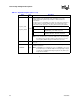
GTLREF0 Input
GTLREF0 determines the signal reference level for GTL+ input signals.
GTLREF0 is used by the GTL+ receivers to determine if a signal is a logical 0 or
logical 1. Contact your Intel representative for further details and
documentation.
GTLREF_SEL Output
GTLREF_SEL is used to select the appropriate chipset GTLREF0 voltage.
Contact your Intel representative for further details and documentation.
HIT#
HITM#
Input/
Output
Input/
Output
HIT# (Snoop Hit) and HITM# (Hit Modified) convey transaction snoop operation
results. Any FSB agent may assert both HIT# and HITM# together to indicate
that it requires a snoop stall, which can be continued by reasserting HIT# and
HITM# together.
Table 4-3. Signal Description (Sheet 1 of 9)
Name Type Description
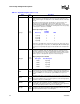
Signals Associated Strobe
D[15:0]#, DBI0# DSTBN0#
D[31:16]#, DBI1# DSTBN1#
D[47:32]#, DBI2# DSTBN2#
D[63:48]#, DBI3# DSTBN3#
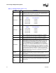
Signals Associated Strobe
D[15:0]#, DBI0# DSTBP0#
D[31:16]#, DBI1# DSTBP1#
D[47:32]#, DBI2# DSTBP2#
D[63:48]#, DBI3# DSTBP3#